Phone

    00852-6915 1330

The Kynix Components - Discrete Semiconductor Products

Stay Ahead with Expert Electronics Insights,
Industry Trends, and Innovative Tips

Discrete Semiconductor Products

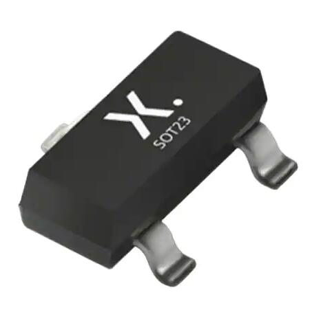
BSS84-7-F P-CHANNEL ENHANCEMENT MODE MOSFET: Datasheet PDF [FAQ]

CatalogProduct SummaryFeatures and BenefitsMechanical DataMaximum RatingsThermal CharacteristicsElectrical CharacteristicsPackage Outline DimensionsSuggested Pad LayoutDatasheet PDF DownloadFAQ Product SummaryBVDSSRDS(on) maxID TA = +25°C50V10Ω @ VGS = -5V-130mA Description and ApplicationsThis MOSFET has been designed to minimize on-state resistance (RDS(on)) and yet maintain superior switching performance, making it ideal for high-efficiency power management applications.General Purpose Interfacing SwitchPower Management FunctionsAnalog Switch Features and BenefitsLow On-ResistanceLow Gate Threshold VoltageLow Input CapacitanceFast Switching SpeedLow Input/Output Leakage Mechanical Data• Case: SOT23 (Standard)• Case Material: UL Flammability Classification Rating 94V-0 • Moisture Sensitivity: Level 1 per J-STD-020• Terminals: Matte Tin Finish (Lead Free Plating) Solderable per MIL-STD-202, Method 208• Terminal Connections: See Diagram• Weight: 0.009 grams (Approximate) Maximum Ratings (@ TA = +25°C, unless otherwise specified.)CharacteristicSymbolValueUnitDrain-Source VoltageVDSS-50VDrain-Gate Voltage RGS £ 20kWVDGR-50VGate-Source Voltage ContinuousVGSS±20VDrain Current (Note 5) ContinuousID-130mAPulsed Drain CurrentIDM-1.2A Thermal Characteristics (@ TA = +25°C, unless otherwise specified.)CharacteristicSymbolValueUnitTotal Power Dissipation (Note 5)PD300mWThermal Resistance, Junction to AmbientRqJA417° C/WOperating and Storage Temperature RangeTJ, TSTG-55 to +150°C Electrical Characteristics (@ TA = +25°C, unless otherwise specified.)CharacteristicSymbolMinTypMaxUnitTest ConditionOFF CHARACTERISTICS (Note 6)Drain-Source Breakdown VoltageBVDSS-50¾¾VVGS = 0V, ID = -250µA Zero Gate Voltage Drain Current IDSS¾¾¾¾¾¾-1-2-100µA µA nAVDS = -50V, VGS = 0V, TJ = +25°C VDS = -50V, VGS = 0V, TJ = +125°C VDS = -25V, VGS = 0V, TJ = +25°CGate-Body LeakageIGSS¾¾±10nAVGS = ±20V, VDS = 0VON CHARACTERISTICS (Note 6)Gate Threshold VoltageVGS(th)-0.8¾-2.0VVDS = VGS, ID = -1mAStatic Drain-Source On-ResistanceRDS(on)¾3.210WVGS = -5V, ID = -0.100AForward TransconductancegFS0.05¾¾SVDS = -25V, ID = -0.1ADYNAMIC CHARACTERISTICS (Note 7)Input CapacitanceCiss¾24.645pF VDS = -25V, VGS = 0V, f = 1.0MHzOutput CapacitanceCoss¾4.725pFReverse Transfer CapacitanceCrss¾2.812pFGate ResistanceRg¾916¾ΩVDS = 0V, VGS = 0V, f = 1MHzTotal Gate Charge (VGS = -4.5V)Qg¾0.28¾nC VDS = -10V, ID = -0.1ATotal Gate Charge (VGS = -10V)Qg¾0.59¾nCGate-Source ChargeQgs¾0.09¾nCGate-Drain ChargeQgd¾0.08¾nCTurn-On Delay TimetD(on)¾10¾nsVDD = -30V, ID = -0.27A, RGEN = 50Ω, VGS = -10VTurn-Off Delay TimetD(off)¾18¾ns    Package Outline Dimensions Suggested Pad Layout Datasheet PDF DownloadYou can download the datasheet from the link given below.BSS84-7-F-Datasheet FAQWhat is P channel enhancement-mode MOSFET?Enhancement-mode MOSFETs are used in integrated circuits to produce CMOS type Logic Gates and power switching circuits in the form of as PMOS (P-channel) and NMOS (N-channel) gates. CMOS actually stands for Complementary MOS meaning that the logic device has both PMOS and NMOS within its design. How does enhancement-mode work in MOSFET?In an enhancement-mode MOSFET, the electrostatic field created by the application of a gate voltage enhances the conductivity of the channel, rather than deplete the channel as in the case of a depletion-mode MOSFET. What is meant by enhancement mode?The switching mosfet that is designed to be in 'OFF' state when the gate voltage applied is zero(i.e. Vs. =0) and will turn on when the gate voltage is pulled to drain voltage(VDD) which is positive voltage for NMOS FETs and Negative for PMOS FETs. View All Products. Engineering Glossary. 
Allen On 2022-07-07   587
Discrete Semiconductor Products

BST82 Transistor Datasheet PDF Donward

CatalogDescriptionFeaturesApplicationsQuick reference dataLimiting valuesThermal characteristicsCharacteristicsPackage outlineDatasheet PDF DownloadFAQ DescriptionN-channel enhancement mode fifield-effect transistor in a plastic package usingTrenchMOS™1 technology.Product availability:BST82 in SOT23. FeaturesTrenchMOS technologyVery fast switchingLogic level compatibleSubminiature surface mount packageApplicationsRelay driverHigh speed line driverLogic level translator Quick reference dataSymbolParameterConditionsTypMaxUnitVDSdrain-source voltage (DC)Tj = 25 to 150 °C-100VIDdrain current (DC)Tsp = 25 °C; VGS = 5 V-190mAPtottotal power dissipationTsp = 25 °C-0.83WTjjunction temperature -150°CRDSondrain-source on-state resistanceVGS = 5 V; ID = 150 mA510WLimiting valuesSymbolParameterConditionsTypMaxUnitVDSdrain-source voltage (DC)Tj = 25 to 150 °C-100VIDdrain current (DC)Tsp = 25 °C; VGS = 5 V-190mAPtottotal power dissipationTsp = 25 °C-0.83WTjjunction temperature -150°CRDSondrain-source on-state resistanceVGS = 5 V; ID = 150 mA510W   Thermal characteristicsSymbolParameterConditionsValueUnitRth(j-sp)thermal resistance from junction to solder pointmounted on a metal clad substrate; Figure 4150K/WRth(j-a)thermal resistance from junction to ambientmounted on a printed circuit board; minimum footprint350K/WTransient thermal impedanceCharacteristics      Package outline Datasheet PDFYou can download the datasheet from the link given below.BST82 Datasheet FAQWhat does a Field Effect Transistor do?FET uses the voltage applied to its input terminal (called the Gate), to control the current flowing from the source to drain, making the Field Effect Transistor a “Voltage” operated device. FETs are extensively used in Integrated Circuits (ICs) due to their compact size and significantly lower power consumption. Why it is called Field Effect Transistor?The value of drain current from the source can be controlled by the potential applied to the gate i.e. the electric field b/w gate and source. That is why such transistor is known as F.E.T. What is the difference between transistor and Field Effect Transistor?BJT and FET are two different types of transistors. Apart from being transistors and both able to do switching as well as amplification, they are quite different from each other. For instance, BJT is a current-controlled current device while FET is a voltage-controlled current device. 
Allen On 2022-06-06   356
Discrete Semiconductor Products

FDC3535 P-Channel Power Trench MOSFET Datasheet PDF Download [FAQ]

CatalogFeaturesGeneral DescriptionApplicationsMOSFET Maximum RatingsElectrical CharacteristicsTypical CharacteristicsDatasheet PDF DownloadFAQ Features„ Max rDS(on) = 183 mΩ at VGS = -10 V, ID = -2.1 A„ Max rDS(on) = 233 mΩ at VGS = -4.5 V, ID = -1.9 A„ High performance trench technology for extremely low rDS(on)„ High power and current handling capability in a widely used surface mount package„ Fast switching speed„ 100% UIL Tested„ RoHS Compliant General DescriptionThis P-Channel MOSFET is produced using ON Semiconductor‘s advanced Power Trench process that has been optimized for rDS(on), switching performance and ruggedness. Applications„ Load Switch„ Synchronous Rectifier MOSFET Maximum RatingsSymbolParameterRatingsUnitsVDSDrain to Source Voltage-80VVGSGate to Source Voltage±20VIDDrain Current  -Continuous (Note 1a)-2.1A-Pulsed-10EASSingle Pulse Avalanche Energy (Note 3)37mJPDPower Dissipation (Note 1a)1.6WPower Dissipation (Note 1b)0.7TJ, TSTGOperating and Storage Junction Temperature Range-55 to +150°C Thermal CharacteristicsRqJCThermal Resistance, Junction to Case30 °C/WRqJAThermal Resistance, Junction to Ambient (Note 1a)78 Package Marking and Ordering InformationDevice MarkingDevicePackageReel SizeTape WidthQuantity.535FDC3535SSOT-67 ’’8 mm3000 units Electrical CharacteristicsSymbolParameterTest ConditionsMinTypMaxUnits Off CharacteristicsBVDSSDrain to Source Breakdown VoltageID = -250 mA, VGS = 0 V-80  VDBVDSSDTJBreakdown Voltage Temperature CoefficientID = -250 mA, referenced to 25 °C -64 mV/°CIDSSZero Gate Voltage Drain CurrentVDS = -64 V, VGS = 0 V  -1mAIGSSGate to Source Leakage CurrentVGS = ±20 V, VDS = 0 V  ±100nA On CharacteristicsVGS(th)Gate to Source Threshold VoltageVGS = VDS, ID = -250 mA-1-1.6-3V DVGS(th) DTJGate to Source Threshold Voltage Temperature CoefficientID = -250 mA, referenced to 25 °C 5 mV/°C rDS(on) Static Drain to Source On ResistanceVGS = -10 V, ID = -2.1 A 147183 mWVGS = -4.5 V, ID = -1.9 A 176233VGS = -10 V, ID = -2.1 A, TJ = 125 °C 246307gFSForward TransconductanceVDD = -10 V, ID = -2.1 A 6.3 S Dynamic CharacteristicsCissInput CapacitanceVDS = -40 V, VGS = 0 V,f = 1 MHz 659880pFCossOutput Capacitance 4965pFCrssReverse Transfer Capacitance 2440pFRgGate Resistance  5.7 W Switching Characteristicstd(on)Turn-On Delay Time VDD = -40 V, ID = -2.1 A, VGS = -10 V, RGEN = 6 W 6.513nstrRise Time 3.110nstd(off)Turn-Off Delay Time 2338nstfFall Time 2.910nsQg(TOT)Total Gate ChargeVGS = 0 V to -10 V VDD = -40 V 1420nCTotal Gate ChargeVGS = 0 V to -4.5 V 6.810nCQgsTotal Gate ChargeID = -2.1 A 1.6 nCQgdGate to Drain “Miller” Charge 2.7 nC Drain-Source Diode CharacteristicsVSDSource to Drain Diode Forward VoltageVGS = 0 V, IS = -2.1 A (Note 2) -0.81-1.3VtrrReverse Recovery TimeIF = -2.1 A, di/dt = 100 A/ms 2540nsQrrReverse Recovery Charge 2338nC Typical Characteristics   Datasheet PDF DownloadYou can download the datasheet from the link given below.FDC3535-Datasheet FAQWhat is power Trench MOSFET?A trench gate MOSFET is basically an attempt to make a complete chip. conduct the current vertically from one surface to the other so as to achieve a high. drive capability. It is realized by packing millions of trenches on a chip, deep. enough to cross the oppositely doped 'body' region below the top surface. What is the difference between MOSFET and power MOSFET?A power MOSFET is a type of MOSFET that is designed specifically to handle high levels of power. These have a high switching speed and can perform much better in low voltage levels than other types of MOSFETs. Its operating principle, however, is similar to that of any other general MOSFET. How much power can a MOSFET handle?Modern MOSFETs can have on resistances of less than 10 milliohms. A little math shows that this device can handle 10 amps with one watt converted into waste heat (power = current2 x resistance). Since many MOSFETs come in TO-220 packages, no heatsink is needed in this instance. 
Kynix On 2022-05-30   371
Discrete Semiconductor Products

BAT54C Schottky Diodes: Datasheet, Pinout, Circuit [FAQ]

Product OverviewPlanar Schottky barrier diodes with an integrated guard ring for stress protection,encapsulated in a small SOT23 (TO-236AB) Surface-Mounted Device (SMD) plastic package. This blog will introduce BAT54C systematically from its features, pinout to its specifications, applications, also including BAT54C datasheet and so much more. CatalogProduct OverviewBAT54C FeaturesBAT54C PinoutBAT54C ApplicationsBAT54C CAD ModelsBAT54C Circuit DiagramBAT54C PackageBAT54C SpecificationBAT54C ManufacturerBAT54C DatasheetUsing WarningsBAT54C FAQ BAT54C FeaturesLow forward voltageLow capacitanceAEC-Q101 qualified BAT54C PinoutThe following figure is the diagram of BAT54C pinout. BAT54C Pinout BAT54C ApplicationsUltra high-speed switchingVoltage clampingLine termination nReverse polarity protection BAT54C CAD ModelsThe following are BAT54C Symbol, Footprint, and 3D Model. BAT54C Symbol BAT54C Footprint BAT54C 3D Model BAT54C Circuit DiagramThe following is the circuit diagram of BAT54C. Reverse Recovery Time Test Circuit and Waveforms BAT54C PackageThe following diagram shows the BAT54C package. BAT54C Package BAT54C SpecificationProduct AttributeAttribute ValueManufacturer:NexperiaProduct Category:Schottky Diodes & RectifiersProduct:Schottky DiodesMounting Style:SMD/SMTPackage / Case:SOT-23-3Configuration:Dual Anode Common CathodeTechnology:SiIf - Forward Current:200 mAVrrm - Repetitive Reverse Voltage:30 VVf - Forward Voltage:800 mVIfsm - Forward Surge Current:600 mAIr - Reverse Current:2 uAMinimum Operating Temperature:- 65 CMaximum Operating Temperature:+ 125 CQualification:AEC-Q101Packaging:ReelPackaging:Cut TapePackaging:MouseReelBrand:NexperiaHeight:1 mmLength:3 mmProduct Type:Schottky Diodes & Rectifiers BAT54C ManufacturerNexperia is a dedicated global leader in discretes, logic and MOSFET devices. Formerly a part of NXP Standard Products, Nexperia is focused on efficiency, producing consistently reliable semiconductor components at high volume. The company’s extensive portfolio meets the stringent standards set by the automotive industry. Industry-leading small packages, produced in Nexperia’s manufacturing facilities, combine power and thermal efficiency with best-in-class quality levels. BAT54C DatasheetYou can download BAT54C datasheet from the link given below:BAT54C Datasheet Using WarningsNote: Please check their parameters and pin configuration before replacing them in your circuit. BAT54C FAQWhat is a Schottky diode used for?Schottky diodes are used for their low turn-on voltage, fast recovery time and low-loss energy at higher frequencies. These characteristics make Schottky diodes capable of rectifying a current by facilitating a quick transition from conducting to blocking state. What is the difference between Schottky diode and normal diode?In the normal rectifier grade PN junction diode, the junction is formed between P type semiconductor to N type semiconductor. Whereas in Schottky diode the junction is in between N type semiconductor to Metal plate. The schottky barrier diode has electrons as majority carriers on both sides of the junction. What is the Schottky diode and how it works?The Schottky Diode is a type of metal-semiconductor diode having a low forward voltage drop and a very fast switching speed. The Schottky Diode is another type of semiconductor diode which can be used in a variety of wave shaping, switching and rectification applications the same as any other junction diode.
Kynix On 2022-05-26   517
Discrete Semiconductor Products

FDN337N Transistor Datasheet PDF Download

CatalogGeneral DescriptionFeaturesAbsolute Maximum RatingsElectrical CharacteristicsTypical Electrical CharacteristicsDatasheet PDF DownloadFAQ General DescriptionSuperSOTTM-3 N-Channel logic level enhancement mode power field effect transistors are produced using Fairchild's proprietary, high cell density, DMOS technology. This very high density process is especially tailored to minimize on-state resistance. These devices are particularly suited for low voltage applications in notebook computers, portable phones, PCMCIA cards, and other battery powered circuits where fast switching, and low in-line power loss are needed in a very small outline surface mount package. Features▪ 2.2 A, 30 V, RDS(ON)= 0.065 W @ VGS = 4.5 V  RDS(ON)= 0.082 W @ VGS = 2.5 V.▪ Industry standard outline SOT-23 surface mount package using proprietary SuperSOTTM-3 design for superior thermal and electrical capabilities.▪ High density cell design for extremely low RDS(ON).▪ Exceptional on-resistance and maximum DC current capability.Absolute Maximum RatingsSymbolParameterFDN337NUnitsVDSSDrain-Source Voltage30VVGSSGate-Source Voltage - Continuous±8VIDDrain/Output Current - Continuous2.2A- Pulsed  10 PDMaximum Power Dissipation (Note 1a) (Note 1b)0.5W  0.46 TJ,TSTGOperating and Storage Temperature Range-55 to 150°CTHERMAL CHARACTERISTICSRqJAThermal Resistance, Junction-to-Ambient (Note 1a)250°C/WRqJCThermal Resistance, Junction-to-Case (Note 1)75°C/WElectrical CharacteristicsSymbolParameterConditionsMinTypMaxUnitsOFF CHARACTERISTICSBVDSSDrain-Source Breakdown VoltageVGS = 0 V, ID = 250 µA30  VDBVDSS/DTJBreakdown Voltage Temp. Coefficient  41 mV/ oCI = 250 µA, Referenced to 25 oC DIDSSZero Gate Voltage Drain CurrentVDS = 24 V, VGS = 0 V  1µA   TJ = 55°C  10µAIGSSFGate - Body Leakage, ForwardVGS = 8 V,VDS = 0 V  100nAIGSSRGate - Body Leakage, ReverseVGS = -8 V, VDS = 0 V  -100nAON CHARACTERISTICS (Note)VGS(th)Gate Threshold VoltageVDS = VGS, ID = 250 µA0.40.71VDVGS(th)/DTJGate Threshold Voltage Temp. Coefficient  -2.3 mV/ oCI = 250 µA, Referenced to 25 oC DRDS(ON)Static Drain-Source On-ResistanceVGS = 4.5 V, ID = 2.2 A 0.0540.065W   TJ =125°C 0.080.11   VGS = 2.5 V, ID = 2 A 0.070.082 ID(ON)On-State Drain CurrentVGS = 4.5 V, VDS = 5 V10  AgFSForward TransconductanceVDS = 5 V, ID = 2.2 A 13 SDYNAMIC CHARACTERISTICSCissInput CapacitanceVDS = 10 V, VGS = 0 V, f = 1.0 MHz 300 pFCossOutput Capacitance  145 pFCrssReverse Transfer Capacitance  35 pFSWITCHING CHARACTERISTICS (Note)tD(on)Turn - On Delay TimeVDD = 5 V, ID = 1 A, 410nsVGS = 4.5 V, RGEN = 6 WtrTurn - On Rise Time  1018nstD(off)Turn - Off Delay Time  1728nstfTurn - Off Fall Time  410nsQgTotal Gate ChargeVDS = 10 V, ID = 2.2 A, VGS = 4.5 V 79nCQgsGate-Source Charge  1.1 nCQgdGate-Drain Charge  1.9 nCDRAIN-SOURCE DIODE CHARACTERISTICS AND MAXIMUM RATINGSISMaximum Continuous Drain-Source Diode Forward Current  0.42AVSDDrain-Source Diode Forward VoltageVGS = 0 V, IS = 0.42 A (Note) 0.651.2VTypical Electrical Characteristics    Datasheet PDF DownloadYou can download the datasheet from the link given below.FDN337N-Datasheet FAQWhat is N-channel transistor?N-Channel MOSFET is a type of metal oxide semiconductor field-effect transistor that is categorized under the field-effect transistors (FET). MOSFET transistor operation is based on the capacitor. This type of transistor is also known as an insulated-gate field-effect transistor (IGFET).What is the function of an transistor?transistor, semiconductor device for amplifying, controlling, and generating electrical signals. Transistors are the active components of integrated circuits, or “microchips,” which often contain billions of these minuscule devices etched into their shiny surfaces. How transistor works as an amplifier?A transistor works as an amplifier by taking in a very small weak signal through the base junction and raising the strength of the weak signal. This amplified signal is released through the collector. 
Kynix On 2022-05-24   371
Discrete Semiconductor Products

IRFB4227PBF Power MOSFET: CAD Models, Datasheet, Features [Video&FAQ]

CatalogProduct OverviewIRFB4227PBF Related Video IntroductionIRFB4227PBF CAD ModelsIRFB4227PBF FeaturesIRFB4227PBF Key ParametersIRFB4227PBF DatasheetIRFB4227PBF SpecificationsIRFB4227PBF ManufacturerUsing WarningIRFB4227PBF FAQ Product OverviewThis HEXFET® Power MOSFET is specifically designed for Sustain¡ Energy Recovery & Pass switch applications in Plasma Display Panels. This MOSFET utilizes the latest processing techniques to achieve low on-resistance per silicon area and low EPULSE rating. Additional features of this MOSFET are 175°C operating junction temperature and high repetitive peak current capability. These features combine to make this MOSFET a highly efficient, robust and reliable device for PDP driving applications. IRFB4227PBF Related Video IntroductionVideo Description: How to measure  “drain-source on resistance” in order to identify a fake MOSFET Transistor. Do this test for your MOSFET and compare it to the datasheet. IRFB4227PBF CAD ModelsFigure: IRFB4227PBF PCB Symbol   Figure: IRFB4227PBF Footprint   Figure: IRFB4227PBF 3D Models IRFB4227PBF FeaturesAdvanced Process TechnologyKey Parameters Optimized for PDP Sustain, Energy Recovery and Pass Switch ApplicationsLow EPULSE Rating to Reduce Power Dissipation in PDP Sustain, Energy Recovery and Pass Switch ApplicationsLow QG for Fast ResponseHigh Repetitive Peak Current Capability for Reliable OperationShort Fall & Rise Times for Fast Switching175°C Operating Junction Temperature for Improved RuggednessRepetitive Avalanche Capability for Robustness and ReliabilityClass-D Audio Amplifier 300W-500W (Half-bridge) IRFB4227PBF Key ParametersKey ParametersVDS max200VVDS (Avalanche) typ.240VRDS(ON) typ. @ 10V19.7m IRP max @ TC= 100°C130ATJ max175°C IRFB4227PBF DatasheetYou can download the datasheet from the link given below:IRFB4227PBF Datasheet IRFB4227PBF SpecificationsTypeDescriptionCategoryDiscrete Semiconductor ProductsTransistors - FETs, MOSFETs - SingleMfrInfineon TechnologiesSeriesHEXFET®PackageTubePart StatusActiveFET TypeN-ChannelTechnologyMOSFET (Metal Oxide)Drain to Source Voltage (Vdss)200 VCurrent - Continuous Drain (Id) @ 25°C65A (Tc)Drive Voltage (Max Rds On, Min Rds On)10VRds On (Max) @ Id, Vgs24mOhm @ 46A, 10VVgs(th) (Max) @ Id5V @ 250µAGate Charge (Qg) (Max) @ Vgs98 nC @ 10 VVgs (Max)±30VInput Capacitance (Ciss) (Max) @ Vds4600 pF @ 25 VFET Feature-Power Dissipation (Max)330W (Tc)Operating Temperature-40°C ~ 175°C (TJ)Mounting TypeThrough HoleSupplier Device PackageTO-220ABPackage / CaseTO-220-3Base Product NumberIRFB4227 IRFB4227PBF ManufacturerInfineon Technologies is a leading global designer, manufacturer and supplier of a broad range of semiconductors used in various microelectronic applications. Infineon's product portfolio consists of logic products, including digital, mixed-signal, and analog integrated circuits, as well as discrete semiconductor products. Using WarningNote: Please check their parameters and pin configuration before replacing them in your circuit. IRFB4227PBF FAQWhat is meant by power MOSFET?A type of metal oxide semiconductor field effect transistor (MOSFET) used to switch large amounts of current. Power MOSFETs use a vertical structure with source and drain terminals at opposite sides of the chip. The vertical orientation eliminates crowding at the gate and offers larger channel widths. What are power MOSFET used for?Power MOSFETs are widely used in transportation technology, which include a wide range of vehicles. In the automotive industry, power MOSFETs are widely used in automotive electronics. Power MOSFETs (including DMOS, LDMOS and VMOS) are commonly used for a wide range of other applications. How does power MOSFET work?Power MOSFETs (Metal-Oxide Semiconductor Field Effect Transistors) are three-terminal silicon devices that function by applying a signal to the gate that controls current conduction between source and drain. What are the important power MOSFET characteristics?Because power MOSFETs are primarily used as power switches, they are expected to have low conduction and switching losses. For power management applications, conduction losses, ruggedness and avalanche capability are important features. Why are MOSFETs used in low power applications?Where the Power MOSFETs are used, it is their low ON resistance that is particularly attractive. This reduces power dissipation which reduces cost and size less metalwork and cooling is required. Also the low ON resistance means that efficiency levels can be maintained at a higher level. 
Kynix On 2022-03-04   672

Kynix

Kynix was founded in 2008, specializing in the electronic components distribution business. We adhere to honesty and ethics as our business philosophy and have gradually established an excellent reputation and credibility in our international business. With the accurate quotation, excellent credit, reasonable price, reliable quality, fast delivery, and authentic service, we have won the praise of the majority of customers.

Follow us

Join our mailing list!

Be the first to know about new products, special offers, and more.

Kynix

  • How to purchase

  • Order
  • Search & Inquiry
  • Shipping & Tracking
  • Payment Methods
  • Contact Us

  • Tel: 00852-6915 1330
  • Email: info@kynix.com
  • Follow Us

authentication

Kynix

© 2008-2026 kynix.com all rights reserve.