Phone

    00852-6915 1330

memory Related Articles

Stay Ahead with Expert Electronics Insights,
Industry Trends, and Innovative Tips

Resistors

What is a Flash Memory Card?

IntroductionFlash memory card, as a high-quality choice for small storage at this stage, has always been favored by consumers due to its many advantages such as good portability, large optional capacity, and plug-and-play. This article will introduce the definition, product type, function, service life and other aspects in detail. CatalogIntroductionRelated Video IntroductionⅠ What is a flash memory card?Ⅱ The Evolution of Flash Memory CardⅢ Types of Flash Memory CardsⅣ Reference Value of the Amount of Data Stored in the Flash Memory CardⅤ What is the Life Expectancy of Flash Memory? (Take the SD CARD as an Example)Ⅵ FAQ about Flash Memory Card Related Video IntroductionVideo: How Does Flash Memory Work?Video Description: In this video, I am going to explain how Flash Memory and Solid-state drives (SSD) work! Have fun, get some popcorn and enjoy! Everybody stores pictures, music, and videos on their devices nowadays. The encoded information is even stored when the device shuts down due to low energy. After powering it on again, we find the same media and are glad that it did not disappear. Flash memory was invented in 1984 by Japanese engineer Fujio Masuoka at the Toshiba Corporation. An electrical storage medium that does not require any energy to retain data. The name "Flash" was suggested by a coworker of Masuoka, Shoji Ariizumi because the erasure process of the newly invented device reminded him of a camera's flash. Later, the invention of flash memory allowed the wide use of solid-state-drives (SSD) that most of us have in their computers today. Ⅰ What is a flash memory card?A flash memory card (also known as a storage card) is a small storage device that stores data on portable or remote computing devices using nonvolatile semiconductor memory. Text, images, audio, and video are examples of such data. The majority of current products use flash memory, but other memory technologies, such as devices that combine dynamic random access memory (DRAM) and flash memory, are being developed. Figure:flash memory card Ⅱ The Evolution of Flash Memory CardAn unknown Toshiba engineer applied for a patent for simultaneous erasable EEPROM in 1980.Perhaps even Dr. Fujio Kaoka didn't realize the value of this patent, let alone the senior Toshiba company, so this cross-epoch patent went unnoticed for four years.Dr. Gang Gang's invention was not made public until 1984, when he presented it at the IEEE International Electron Devices Meeting (IEDM) in San Francisco, California.Intel recognized the enormous potential of this invention at the conference and released the first commercial NOR Flash chip in 1988. (the original CompactFlash was originally based on NOR Flash, although it later switched to a lower-cost NAND Flash.) The story does not end there. Dr. Fujio Kaoka discovered that NOR Flash has a long erasure time and thus invented NAND Flash in 1986. NAND Flash has a faster erasing time and a smaller area for each memory cell than NOR Flash, giving it a higher storage density and lower cost per bit. Since then, flash memory (both NOR and NAND) has been created. The irony is that despite his significant contribution, he only received a few hundred dollars in Toshiba rewards and a high-ranking but laid-back position. He couldn't take this kind of treatment as an engineer and had to resign and enroll in university to continue his scientific research. Memory cards based on NAND Flash were later developed. SmartMedia was the first application of NAND Flash. Since then, NAND Flash has been adopted by a wide range of storage media. Ⅲ Types of Flash Memory CardsMultimedia Card,A Multimedia Card is a type of flash memory card. Its size is 32mm 24mm 1.4mm and weight is 1.5 grams, making it ideal for digital imaging, music, mobile phones, PDAs, e-books, toys, and other products. However, due to a lack of support from consumer digital manufacturers, there aren't many products in the digital product market that can use MMC memory cards.Figure:Multimedia Card Panasonic, Toshiba, and SanDisk of Japan collaborated to develop the SD card (Secure Digital). It is 32mm24mm2.1mm in size and weighs only 2 grams, but it has a large capacity, a high data transmission rate, and good flexibility. The SD card's structure ensures the security of digital file transfer, and it is simple to reformat, so it has a wide range of applications. SD cards are widely used as storage media in digital cameras. As a result, the SD card is the most widely used memory card.Figure:SD Card Mini SD cards are derived from SD cards, and their performance is comparable to that of standard SD cards. Mini SD cards, like SD cards, have a hardware data write protection switch to prevent accidental deletion of stored content. The Mini SD card, on the other hand, is 40 percent smaller than the SD card, measuring only 21.5 mm20 mm1.4mm. It is fully compatible with standard SD card slots and can be used with a dedicated adapter card.Figure:Mini SD Card The most important difference, however, is that the Mini SD card uses a low-power design, making it more suitable for mobile communication equipment than the SD card. It is currently used primarily in information terminal equipment such as mobile phones, PDAs, and handheld computers. T-Flash card, full name: TransFLash (also: Micro SD), is a very small flash memory card developed and launched jointly by Motorola and SANDISK. It has the advantage of being small and is primarily used in mobile phones, but as capacity increased, it gradually began to be used in a broader range of fields. At the same time, it has a large capacity and can be connected to the SD card slot via an adapter.Figure:T-Flash Card Memory Stick is the full name of a mobile storage medium developed by Sony Corporation of Japan. This type of storage device resembles chewing gum and has a high level of compatibility. Later, Sony reduced the volume based on the memory stick to about one-third and designed and manufactured the memory stick Duo. This type of memory stick Duo is ideal for use in small mobile phones and digital cameras, as well as various mp3 players and other electronic devices.Figure:Memory Stick The latest bus and interface standard is PCI-e flash memory card (PCI-Express). It was originally known as "3GIO." PCIe is a serial point-to-point dual-channel high-bandwidth transmission standard. Exclusive channel bandwidth is assigned to the connected devices. Shared resources, primarily supporting functions such as active power management, error reporting, end-to-end reliability transmission, hot plug, and service quality (QOS). The concept is based on NAND flash memory.Figure:PCI-e Flash Memory Card CF cards (Compact Flash) were originally used in portable electronic devices as a data storage device. It revolutionized the use of flash memory as a storage device, which was first produced by SanDisk in 1994 and formulated relevant specifications. Many devices are currently using its physical format. However, the CF card's capacity is limited, and increasing its capacity cannot keep up with the development of digital camera pixels. The size is relatively large when compared to other types of memory cards, and the operating temperature is generally 0-40 degrees Celsius, which limits its performance.Figure:CF Card Sony's XQD memory card is a type of memory card. It is much smaller than a standard CF card, only about half the size. The XQD memory card, on the other hand, retains the CF card's fast and stable reading. Furthermore, the XQD memory card employs an upgradeable high-performance interface. It had a read and write speed of 125 megabits per second.Figure:XQD Memory Card Olympus and Fuji jointly launched the XD-Picture Card (xD) memory card. It has an extremely small external size of 20mm25mm1.7mm and a weight of only 2 grams. Its read and write speeds can reach 5MB/S and 3MB/S, respectively. Initially, the XD card was primarily used in Olympus and Fuji digital camera products. Despite the fact that its performance can meet the requirement of writing large amounts of data and its power consumption is lower, the relatively high price has severely limited the development of XD cards. Olympus and Fuji digital cameras no longer exclusively use XD cards as storage media.Figure:XD Card The M2 card is a new Memory Stick Micro (M2) memory card jointly released by Sony and SanDisk. It debuted in March 2006. This type of M2 card uses an ultra-small circuit design, specifically for large-capacity, small-volume mobile storage needs; it weighs only 16 grams, has dimensions of only 15 12.5 1.2mm, and has a volume roughly one-fourth that of a memory stick Pro Duo.Figure:M2 Card  Ⅳ Reference Value of the Amount of Data Stored in the Flash Memory Card PhotosVideosMusice-books                          FormatStorage JPEG(10MP)MP4(minutes)MP3PDF(10MB)16GB320810883040163832GB641621766080327664GB128324352121606553128GB2566487042432013107256GB51328174084864026214  Ⅴ What is the Life Expectancy of Flash Memory? (Take the SD CARD as an Example)An SD card is a solid-state device, which means it has no moving parts. This is a significant advancement over older portable storage devices, such as floppy disks, which had thin, flimsy disks spinning at high speeds. The components of an SD card are part of its circuitry, which is why they are so small and compact. Data is stored on flash memory chips found on circuitry. Flash memory is a type of EEPROM chip (Electrically Erasable Programmable Read Only Memory). There are two types of memory cells used in solid-state devices such as SD cards. Lots of SD cards employ single-level memory cells that are either turned on or off. Because these cells can only store a single value, they are fast and dependable. The disadvantage is that you need a large number of them in a large memory card. Most low-cost SD cards use multi-level cell chips. Each cell stores a voltage, and the level of the voltage represents a range of values. Memory cells are insulated to prevent charge leakage. This insulation, however, is eroded each time a write action is performed. This can cause the voltage in a cell to fluctuate slightly over time, causing the data on the SD card to become corrupted. Most modern SD cards are designed to detect and avoid these problem cells, but if there are too many, the card may not have enough memory to map them over time. The exact lifespan of an SD card is determined by a number of factors. If you use your card on a regular basis, it should last a long time assuming it doesn't physically break first. For example, if you use it more than once a week, it's a good idea to replace it once a year.Due to the various pressures people put on SD cards, determining when to replace them is difficult. Most likely, your SD card will physically stop working due to damage before it begins corrupting your data. SD cards are made with low-cost components to keep costs low, and as a result, they are prone to breaking. SD cards are definitely not suitable for long-term storage due to the charge in the cells leaking over time. Although there are special SD cards designed to be written to only once and used for archival purposes, commercially available SD cards such as those found in cameras should not be used in this manner. Most SD cards will not keep data for more than five years. The best way to keep your data safe is to copy it as soon as possible from your SD card to your computer. Ⅵ FAQ about Flash Memory Card1. What are the benefits of flash memory?Increased Durability. Unlike traditional hard-disk drives, flash drives lack moving parts, maximum Portability, plenty of Storage Capacity,Fast Transfer Speeds, compatibility with Many Devices, use Flash Drives as Promotional Materials. 2. Why do smartphones use flash memory?Flash memory is non-volatile computer memory that can be electrically erased and reprogrammed. It's used as primary storage memory on various portable devices due to its low cost, compact size, great physical endurance and low power consumption. 3. Is Flash Memory expensive?Traditional storage drives cost about 7 or 8 cents per usable gigabyte, while flash storage drives cost about 40 cents per usable gigabyte. The price of solid-state drives (SSDs) is falling, but the price of flash storage is declining even faster. 4. What is the difference between flash and EEPROM memory?Flash memory is a distinct type of EEPROM, which is programmed and erased in large blocks. Flash uses NAND-type memory, while EEPROM uses NOR type. Flash is block-wise erasable, while EEPROM is byte-wise erasable. Flash is constantly rewritten, while other EEPROMs are seldom rewritten. 5. How reliable is a flash memory card?Today most commercially available flash memory is guaranteed to withstand 100 000 or more programme-erase cycles with some manufacturers guaranteeing a life of over 1 000 000 cycles. 
kynix On 2021-08-24   5614
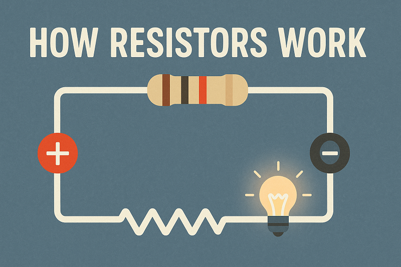
Resistors

Types of Flash Memory Comparison: NAND vs NOR

IntroductionFLASH is a type of non-volatile memory that retains data even when power is disconnected. Unlike RAM, which can rewrite data at the byte level, flash memory operates differently. A flash memory chip consists of an array of data storage cells organized into blocks, with each block containing multiple pages (typically 64 to 256 pages in modern devices, though older devices used 32 pages). A page is usually 2KB, 4KB, 8KB, or 16KB in modern NAND flash, though the original specification was 512 bytes plus spare area, as flash was initially developed as a disk replacement technology.What Is Flash Memory?Ⅰ Types of Flash MemoryFlash memory is widely used as a storage medium in digital cameras, smartphones, tablets, USB drives, SSDs, and various consumer electronics. Flash memory cards come in various form factors depending on manufacturers and applications, including USB flash drives, CompactFlash (CF card), MultiMediaCard (MMC card), Secure Digital (SD card, microSD), Memory Stick, and XD-Picture Card (XD card). Note that SmartMedia (SM card) and Microdrive have been discontinued. While these flash cards have different physical formats and specifications, their underlying technical principles remain similar.Flash memory includes two main architectural types: NOR Flash and NAND Flash. NOR Flash is a random access device with dedicated address and data lines (similar to SRAM), allowing byte-level read and write operations and direct access to any memory location, making it an excellent ROM alternative, such as in computer BIOS chips. NAND Flash, however, lacks dedicated address lines and cannot be directly addressed. It is controlled by sending commands and addresses through an I/O interface, meaning NAND Flash can only be accessed in pages, making it more suitable for sequential data storage.Ⅱ NAND Flash MemoryNAND Flash is extensively used in high-capacity storage devices such as memory cards, USB drives, SSDs, eMMC, and UFS storage. NAND Flash cells are categorized by the number of bits stored per cell: SLC (Single-Level Cell), MLC (Multi-Level Cell), TLC (Triple-Level Cell), and QLC (Quad-Level Cell). SLC stores 1 bit per cell, MLC stores 2 bits, TLC stores 3 bits, and QLC stores 4 bits per cell.As more bits are stored in a single cell, the read/write performance decreases, endurance diminishes, but cost per gigabyte is reduced, making higher-density options more economical for consumer applications.ItemsSLCMLCTLCQLCBits Per Cell1234P/E Cycles50,000-100,0003,000-10,0001,000-3,000100-1,000Read Time (μs)255075100Program Time (μs)200-300600-900900-13501350-2000Erase Time (ms)1.5-234.56-8SLC is primarily used in enterprise, industrial, and military applications due to its high-speed writing, low error rate, and exceptional durability.MLC is targeted at consumer and prosumer applications, offering twice the capacity of SLC at lower cost. It's suitable for USB drives, smartphones, digital cameras, and consumer-grade SSDs.TLC has become the mainstream choice for consumer SSDs and SD cards due to its balance of cost, capacity, and acceptable performance for everyday use.QLC, introduced more recently, offers even higher density and lower cost per gigabyte, making it increasingly popular in budget SSDs and high-capacity storage solutions, though with reduced endurance.As a practical solid-state storage medium, NAND Flash has unique physical characteristics requiring specialized management. Designers face several key challenges:1) Erase-before-write requirement: Data cannot be overwritten directly; blocks must be erased before new data can be written2) Wear mechanism: Limited program/erase (P/E) cycles impose durability constraints3) Read/write interference: Operations can cause data errors in adjacent cells4) Data retention: Charge leakage over time can cause data loss5) Bad block management: Both factory defects and runtime failures must be managedKey technologies addressing these challenges include:1) Cell type selection: Choosing appropriate NAND type (SLC/MLC/TLC/QLC) based on application requirements2) Wear leveling algorithms: Distributing write operations evenly across all blocks to maximize lifespan3) Bad block management: Identifying and mapping out defective blocks to ensure data integrity4) Error Correction Code (ECC): Detecting and correcting bit errors using advanced algorithms like BCH or LDPC5) Write amplification mitigation: Minimizing unnecessary write operations to extend device life6) Garbage collection: Consolidating valid data and reclaiming space from partially used blocksData is stored as electrical charge in Flash memory cells. The amount of stored charge depends on the voltage applied to the Control Gate, which controls whether charge is injected or removed from the floating gate.1) For programming (writing) NAND Flash, voltage is applied to the Control Gate to inject electrons into the floating gate. When charge exceeds the threshold voltage (Vth), the cell represents a logical 0.2) For erasing NAND Flash, electrons are removed from the floating gate. When charge falls below the threshold voltage (Vth), the cell represents a logical 1. Ⅲ NOR Flash MemoryNOR Flash, similar to conventional memory, supports random access, enabling XIP (eXecute In Place) functionality. This allows code execution directly from the flash without copying to RAM, making it ideal for boot code, BIOS/UEFI firmware, and embedded system applications requiring immediate code execution.NOR Flash is categorized into two types based on host interface: Parallel NOR Flash and Serial NOR Flash.Parallel NOR Flash connects directly to the host controller with its contents mapped into the CPU address space, eliminating the need to copy to RAM. Early BIOS implementations used the FWH (Firmware Hub) interface, a parallel connection that has been largely obsoleted due to pin count and speed limitations.Serial NOR Flash is more cost-effective than Parallel NOR Flash and typically connects to the host processor or Platform Controller Hub (PCH) via SPI (Serial Peripheral Interface), Quad-SPI (QSPI), or Octal-SPI interfaces. Modern implementations support higher speeds through multi-lane configurations.Today, virtually all UEFI/BIOS firmware, embedded systems, IoT devices, and many consumer electronics use NOR Flash. Typical capacities range from 1MB to 256MB, with 16MB-128MB being common for modern UEFI implementations. While more expensive per gigabyte than NAND, NOR Flash offers superior reliability and random access performance.NOR Flash has slower erase speeds and lower erase cycle counts compared to NAND, but these limitations rarely impact BIOS/firmware performance or cause device failures due to the infrequent update nature of firmware. Ⅳ NAND Flash vs NOR FlashCompared with NOR flash memory, NAND flash memory requires fewer transistors per cell to store the same amount of data, resulting in smaller die size and higher storage density. This architectural difference makes NAND significantly more cost-effective for high-capacity storage applications.In terms of read speed, NOR flash memory offers faster random access than NAND flash memory, with typical access times of 50-100ns compared to NAND's page-based access. However, NAND flash memory significantly outperforms NOR in sequential write and erase operations. NAND's block-based erase operation is simpler and faster, erasing entire blocks (typically 128KB-4MB) at once.NOR flash memory requires all bits to be set to 1 during erase operations before programming. While NOR flash memory provides faster random access and simpler byte-level operations, its lower storage density and higher cost make it more suitable for code storage and execution. NAND flash memory provides extremely high cell density (modern single chips can exceed 1TB capacity), making it ideal for mass data storage with fast write and erase speeds. Additionally, NAND flash operates on page-based read/write units (typically 4KB-16KB) and block-based erase units, making it functionally similar to traditional disk drives.NAND Flash is more susceptible to bit errors than NOR Flash, necessitating robust Error Detection and Correction (EDC/ECC) algorithms. Modern NAND implementations use advanced ECC schemes like BCH (Bose-Chaudhuri-Hocquenghem) or LDPC (Low-Density Parity-Check) codes. Additionally, NAND Flash develops bad blocks over its lifetime. File systems like FAT on SD cards experience frequent rewrites of the file allocation table, and the P/E cycle count per block is critical to NAND Flash longevity. Balancing erase cycles across all blocks and managing bad blocks requires specialized firmware-level functionality including bad block management, wear leveling, ECC, and garbage collection. This management layer is called the FTL (Flash Translation Layer). Based on FTL implementation location, Flash Memory is categorized as Raw Flash or Managed Flash.Raw Flash requires the host system to implement FTL functionality, giving designers complete control but requiring significant software development. Managed Flash (such as eMMC, UFS, SD cards) includes an integrated controller that handles FTL operations transparently, simplifying host system design at the cost of reduced low-level control.Ⅴ Universal Flash Storage Versions ComparisonStorage performance significantly impacts device responsiveness and user experience. Universal Flash Storage (UFS) has become the dominant standard for high-performance mobile and embedded storage, replacing the older eMMC standard. UFS provides a standardized flash storage specification optimized for smartphones, tablets, automotive systems, and other performance-critical applications. Version numbers indicate generational improvements, with higher versions offering substantially better performance, features, and efficiency.✔️Version Comparison (Main Parameters)UFS Version1.01.12.02.13.03.14.0Introduced2011-02-242012-06-252013-09-182016-04-042018-01-302020-01-302023-09-14Bandwidth per lane300 MB/s600 MB/s1450 MB/s (HS-G3)2900 MB/s (HS-G4)5800 MB/s (HS-G5)Max. number of lanes12Max. total bandwidth300 MB/s1200 MB/s2900 MB/s (HS-G3)5800 MB/s (HS-G4)11600 MB/s (HS-G5)M-PHY version1.03.04.15.0UniPro version1.41.61.82.0✔️UFS 2.1 vs UFS 2.2The primary enhancement in UFS 2.2 over UFS 2.1 is the Write Booster feature, which significantly improves write performance. Write Booster uses SLC (Single-Level Cell) cache to accelerate write operations, providing faster application launches, improved browser cache loading, reduced video encoding times, and enhanced overall system responsiveness. This feature is particularly beneficial for burst write scenarios common in mobile devices.As eMMC has been phased out from mainstream consumer devices and NAND flash prices have decreased, UFS adoption has accelerated. UFS 2.2 briefly served as a transitional standard before UFS 3.x became mainstream in flagship devices.✔️UFS 3.0 vs UFS 3.1UFS 3.1 introduces three significant enhancements over UFS 3.0:1) Write Booster (Enhanced)Write Booster in UFS 3.1 is an enhanced version that increases device write speed substantially. This feature can boost write speeds up to 700 MB/s, compared to UFS 3.0's typical sequential write performance of around 500 MB/s. The mechanism works similarly to SLC caching in SSDs: a portion of TLC/QLC storage is dynamically configured to operate in SLC mode, providing faster write performance. Data is initially written to this high-performance buffer, then migrated to standard storage during idle periods, freeing the cache for subsequent operations.2) Deep Sleep ModeDeep Sleep enables the flash memory to enter an ultra-low-power state during extended idle periods, significantly reducing standby power consumption. This feature helps extend battery life during device standby and contributes to overall device thermal management. Deep Sleep can reduce idle power consumption by up to 40% compared to standard sleep modes.3) Host Performance Booster (HPB)HPB addresses long-term performance degradation by improving random read performance. As devices are used over time, file system fragmentation and the need to frequently reload the Logical-to-Physical (L2P) mapping table can cause performance degradation. HPB leverages the host device's RAM to cache portions of the L2P mapping table, reducing latency for random read operations. This is particularly effective at maintaining consistent performance after extended use, preventing the "slowdown over time" phenomenon common in storage devices. HPB can improve random read IOPS by up to 70% in fragmented scenarios.✔️UFS 4.0 - The Latest GenerationReleased in September 2023, UFS 4.0 represents the latest advancement in mobile storage technology. Key improvements include:• Doubled bandwidth: Up to 11.6 GB/s (5800 MB/s per lane with dual-lane configuration) using HS-G5 gear• Improved power efficiency: Lower power consumption per bit transferred compared to UFS 3.1• Enhanced thermal management: Better heat dissipation characteristics for sustained performance• Advanced features: Builds upon Write Booster, Deep Sleep, and HPB with further optimizationsUFS 4.0 is designed for next-generation flagship smartphones, tablets, and high-performance mobile devices requiring extreme storage bandwidth for 8K video recording, advanced computational photography, and AI workloads. Frequently Asked Questions about Flash Memory1. What are the different types of flash memory?Flash memory comes in two fundamental architectural types: NOR and NAND. NOR flash offers random access and execute-in-place capabilities, making it ideal for code storage. NAND flash provides higher density and faster write speeds, making it suitable for data storage. Within NAND flash, there are further subdivisions based on bits per cell: SLC (1 bit), MLC (2 bits), TLC (3 bits), and QLC (4 bits), each offering different trade-offs between performance, endurance, and cost. 2. What are the characteristics of flash memory?Flash memory has several distinctive characteristics: it is significantly less expensive than EEPROM and doesn't require batteries for data retention unlike SRAM. It is non-volatile, meaning data persists without power. Flash offers fast read access times (microseconds), high resistance to physical shock compared to hard disk drives, low power consumption, and silent operation. However, it has limitations including finite write/erase cycles, block-level erase requirements, and potential for bit errors requiring ECC. 3. What is the purpose of flash memory?Flash memory serves as a non-volatile storage solution widely used in embedded systems, consumer electronics, and enterprise storage. It retains data without power, can be electrically erased and reprogrammed, and offers advantages over traditional magnetic storage including faster access times, lower power consumption, better durability, and compact form factors. Flash memory evolved from EEPROM technology and has become the dominant storage technology for mobile devices, SSDs, USB drives, memory cards, and embedded systems. 4. What is the difference between NAND flash and NOR flash?NOR flash provides faster random read access and supports execute-in-place (XIP), allowing direct code execution without copying to RAM, making it ideal for firmware and boot code. However, it's more expensive and has slower erase/write operations. NAND flash offers higher storage density, lower cost per gigabyte, and much faster sequential write and erase speeds, making it ideal for mass storage applications. NAND is accessed serially through a shared I/O interface, while NOR has parallel address and data buses allowing random access. NAND requires more complex error correction due to higher bit error rates. 5. What is the difference between UFS and eMMC?UFS (Universal Flash Storage) is the successor to eMMC (embedded MultiMediaCard) and offers several significant advantages: UFS supports full-duplex operation allowing simultaneous read and write operations, while eMMC is half-duplex. UFS uses a faster serial interface with higher bandwidth (up to 11.6 GB/s in UFS 4.0 vs. 400 MB/s in eMMC 5.1). UFS also features command queuing for better multitasking performance, lower latency, and improved power efficiency. These advantages make UFS the preferred choice for modern flagship smartphones and high-performance mobile devices. 6. How does wear leveling work in flash memory?Wear leveling is a technique used to extend flash memory lifespan by distributing write and erase cycles evenly across all memory blocks. Since flash memory has a limited number of program/erase cycles per block, repeatedly writing to the same blocks would cause premature failure. Wear leveling algorithms track the erase count of each block and preferentially use blocks with lower erase counts for new writes. This ensures all blocks wear out at approximately the same rate, maximizing the overall device lifespan. Modern flash controllers implement sophisticated wear leveling algorithms as part of the Flash Translation Layer (FTL). 7. What is 3D NAND technology?3D NAND (also called V-NAND) is a flash memory architecture that stacks memory cells vertically in multiple layers, rather than arranging them in a single planar layer. This technology allows for higher storage densities without requiring smaller manufacturing process nodes. Modern 3D NAND implementations can have over 200 layers, significantly increasing capacity while improving performance and endurance compared to planar NAND. 3D NAND also offers better power efficiency and can achieve higher performance due to reduced cell-to-cell interference. This technology has become the standard for modern SSDs and high-capacity storage devices.
Kynix On 2021-07-19   5098
Resistors

ECC Memory or Not for Computer Server? ECC Server RAM

IntroductionAs everyone knows, Error correction code memory (ECC memory) is a type of computer data storage technique. It identifies and fixes the most common errors which could otherwise lead to data corruption or system crashes. In other words, it is one of the most important techs for this loss and system errors prevention. There will be people who have such a question: now the memory technology is improved greatly, it’s possible to use ECC server RAM inside of your regular desktop computer at home, but is it something you SHOULD do? This note will help you find clues step by step.ECC Memory ExplainedCatalogIntroductionⅠ What Causes Errors in RAM?Ⅱ Is ECC RAM Better?Ⅲ ECC Server RAM or Regular Home Desktop?Ⅰ What Causes Errors in RAM?The ram error is caused by electromagnetic interference inside the computer. This interference will cause the units of DRAM (Dynamic Random Access Memory) to spontaneously change to the opposite state. Unit errors may be hidden, that is, they will not have a serious impact on the data. However, the memory units are interrelated, so unit changes may affect the entire operating system, resulting in system errors, especially when the strict operation is required. To be specific, memory errors will cause security vulnerabilities, crashes, transcription errors, lost transactions and corrupted or lost data, and one of the most common types of memory error is a single-bit error.Ⅱ Is ECC RAM Better?In the face of these problems, if memory can fix the error itself, what will it look like? That is ECC RAM.Memory Chips DifferenceECC RAM is server memory. This type of memory module has an ECC error check storage chip (the number of storage chips is an odd number). The application of ECC can ensure that the server is safer and more stable during operation. However, the number of chips stored in ordinary memory sticks is even. In reality, ECC RAM has 9 memory chips instead of 8. Error Checking and CorrectingThe ECC memory is equipped with ECC error-checking technology. After error checking and correction, the stability and reliability of the server system can be effectively guaranteed. For ordinary ram, when the word detects an error, the error location cannot be determined, and the error cannot be corrected. Therefore, for a single task that takes a long time and cannot be suspended or error, ECC memory is an inevitable choice. However, ordinary PCs will not use because of high-cost price. Application DifferenceBecause ECC memory can effectively store and maintain data integrity and is equipped with check and correction technology, ECC memory further reduces data corruption. Therefore, it is mostly used in servers and graphics workstations such in financial and scientific industries. Non-ECC memory sticks are more suitable for the general public's use. Capacitor DifferenceAs server memory applications require higher capacity, ECC memory modules usually start at 4GB, while ordinary memory modules usually start at 2GB. The standard configuration on home computers is 4~8GB of memory. Price DifferenceDue to the higher-tech of ECC memory sticks, their capacity is also larger than ordinary memory. Therefore, ECC memory sticks are more expensive than ordinary memory.Ⅲ ECC Server RAM or Regular Home Desktop?ECC memory is usually used in servers or graphics workstations. Because of the check and correction function, when there are some read and write errors in the memory, the ECC RAM can correct these errors and reduce the probability of downtime/blue screen. Guaranteed data storage and accuracy of reading and writing.Server memory and ordinary PC memory are very similar, there is no obvious difference in appearance and structure, but its price is higher than ordinary memory. There are three main types of server memory: SDRAM, DDR, and DDR2. At present, server memory is mostly used by DDR and DDR2. As time goes by, the server uses some new technologies now, such as ECC, chip kill, register, hot-swap technology, FB-DIMM (full buffer memory module), etc. More server memory currently adopts ECC and REG ECC technologies. The chips on REG ECC memory are generally 2-3 more than ordinary motherboards, mainly PLL (phase-locked loop) and Register IC. ECC and ECC REG memory have been developed for a period, and the frequency mainly has 133, 266, 333, 400, 533, and 667 stages. What is RECC? The specific uses of RECC memory are as follows: phase-locked loop chip, the bottom of the memory stick are smaller than Register ICs. Generally, there is only one, which can adjust the clock signal and ensure signal synchronization between the memory modules. The smaller IC chip (2-3 pieces) at the bottom plays a role in improving the driving capability. Server products need to support large-capacity memory. The motherboard alone cannot drive such a large-capacity memory. Instead, the memory module with Register is used to improve the driving ability, so that the server can support up to 32GB of memory. Because of the PLL and Register chips, the server memory capacitor can be made very large, it can better meet the endless requirements of the ever-increasing software for memory. Therefore, it is recommended that the server whose requirement is over 16G use RECC RAM.RECC has one more register. We can understand the function of the memory as a book directory. When the memory receives a read and write command, it will retrieve this directory first, and then perform read and write operations, which will greatly improve the efficiency of the server memory. So some people mistakenly think that RECC RAM runs slower than ECC RAM. The Register memory that can be used at present also has an ECC function, and some motherboards require the memory to support Register. In fact, all registered memory is ECC memory. The use of ECC memory requires the support of other computer components, such as the motherboard and cpu, and may also need to be set in the BIOS before it can be used on most server CPUs and motherboards (some non-server CPUs and motherboards also support). In addition, when purchasing ecc memory, you need to pay attention to whether it is ecc udimm or ecc rdimm or ecc lrdimm or ecc 3ds rdimm or something else. Because your computer configuration may not support some types.What’s more, all of the modern, contemporary storage drives use ECC at some level internally. HDD, SSDs. The data densities of the HDD push the edge where need to keep up with track integrity. NAND in SSDs tend to loose data bits in usage over time. The SSD controller in the T2 isn't remarkable on the ECC dimension. All the ones that store the data encrypted 'at rest' basically have to if going to be competently implemented. In addition, ECC generally works on all Ryzen Chips minus the APUs (with the exception of the pro apus), they tend to not be on the QVL since it costs time and money to do that. Frequently Asked Questions about ECC Server Memory1. What is ECC memory?Error correction codeError correction code (ECC) memory is a type of RAM memory found in workstations and servers. It's valued by professionals and businesses with critical data for its ability to automatically detect and correct memory errors, thus fighting data corruption. 2. Which is better ECC or non-ECC memory?Non-ECC (also called non-parity) modules do not have this error-detecting feature. ... Using ECC decreases your computer's performance by about 2 percent. Current technology DRAM is very stable, and memory errors are rare, so unless you have a need for ECC, you are better served with non-parity (non-ECC) memory. 3. How does ECC memory work?ECC memory uses the extra bits to store an encrypted code when writing data to memory, and the ECC code is stored at the same time. ... As data is processed, ECC memory is constantly scanning code with a special algorithm to detect and correct single-bit memory errors. 4. What is the benefit of ECC memory?ECC memory protects your system from potential crashes and inadvertent changes in data by automatically correcting data errors. This is achieved with the addition of a ninth computer chip on the RAM board, which acts as an error check and correction for the other eight chips. 5. Who needs ECC RAM?Error-correcting code memory (ECC memory) is a type of computer data storage that can detect and correct the most common kinds of internal data corruption. ECC memory is used in most computers where data corruption cannot be tolerated under any circumstances, such as for scientific or financial computing.
kynix On 2021-05-25   6257
Resistors

In-Memory Computing Technology Overview

IntroductionIn-memory computing (IMC), a technique of future computing, stores data in RAM to run calculations entirely in computer memory. With the rise of the big data era, faster data processing capabilities are required. Computer memory and storage space are also growing exponentially to adapt to large-capacity data collection and complex data analysis, which promotes the development of AI (artificial intelligence), and then derives emerging stuff, that is, in-memory computing.In-memory Computing (IMC) ExplainedCatalogIntroductionⅠ Memory Wall: Processor /Memory Performance GapⅡ Developing RequirementⅢ What Is In-memory Computing?3.1 In-memory Computing Definition3.2 Four Realization MethodsⅣ Driving Force of In-memory Computing and Market Prospects4.1 In-memory Computing for AI4.2 In-memory Computing Product Outlook4.3 In-memory Computing Market and ProspectⅤ ConclusionⅠ Memory Wall: Processor / Memory Performance GapThe von Neumann architecture has occupied the dominant position in computer system when the computer invented. This kind of calculation method is to store the data in the main memory first, and then fetch the instructions from the main memory to execute them in order when running. We all know that if the connecting speed of the memory cannot keep up with the performance of the CPU, the computing will be limited. This is a memory wall. At the same time, in terms of efficiency, the von Neumann architecture also has obvious shortcomings. It consumes more energy to read and write data than to calculate once time.Figure 1. Von Neumann Architecture DiagramThe performance of computer processors has developed rapidly based on Moore's Law, and has been directly improved with the invention of transistors. The main memory of the computer uses the DRAM. It is a high-density storage solution based on capacitor charging and discharging. Its performance (speed) depends on two aspects, namely the reading/writing speed of the capacitor charging and discharging in the memory and the interface bandwidth between the devices. The read/write speed of capacitor charging and discharging has increased with Moore’s Law, but the speed is not as fast as the processor. In addition, the interface between DRAM and the processor is a mixed-signal circuit, and its bandwidth increasing speed is mainly restricted by the signal integrity of the traces on the PCB. This has also caused the performance improvement of DRAM to be much slower than that of the processor. At present, the performance of DRAM has become an huge bottleneck of overall computer performance, the so-called "memory wall".  It blocks the computing performance improvement.Figure 2. Moore's Law Effect Ⅱ Developing RequirementIn the current AI technology, with the increasing amount of data and calculations, the original von Neumann architecture is facing more and more challenges. Rely on expanding CPU, the hardware architecture can’t have a large amount of calculation. Also the larger storage capacity is heavily rely on the past architecture, it is also very unsuitable for AI. When the memory capacity is large to a certain extent, it can only show that certain technologies need innovation. In order to solve the "memory wall" problem, future computers are not based on computing memory, but the in-memory computing, thereby reducing the cost of data access in the calculation process.Figure 3. Conventional Computing vs In-memory Computing Ⅲ What Is In-memory Computing?3.1 In-memory Computing DefinitionIn-memory computing (or in-memory computation) is a technique based on RAM data storage and indexing, which proposed by the MIT research group, and its main purpose is to accelerate the convolution calculation. We know that convolution calculations can be expanded into weighted accumulation calculations. From another perspective, it is actually a weighted average of multiple numbers. Therefore, the circuit realizes the weighted average of the charge domain. The weight (1-bit) is stored in SRAM, and the input data (7-bit digital signal) becomes an analog signal through the DAC. According to the corresponding weight in the SRAM, the output is multiplied by 1 or -1 in the analog domain, which averaged in the analog domain, and finally read out by the ADC as a digital signal. Specifically, since the weight of the multiplication is 1-bit (1 or -1), it can be controlled by using a switch and a differential line simply. If the weight is 1, the capacitor on the side of the differential line is charged to the required output value. Otherwise, let the other side of the differential line be charged to this value. As for average, connect several differential lines together in the charge domain.Of course, there is more than one circuit for in-memory calculation, and the calculation accuracy is not limited to 1-bit. However, we can see the above examples that the core idea of in-memory calculations is generally to convert calculations into weighted calculations. Store the weights in the memory unit, then modifications on the core circuit of the memory (such as the readout circuit) are made. So that the process of reading is like a process in which the input data and weights are multiplied in the analog domain, that is, convolution. Because convolution is a core part of AI and other calculations, in-memory computing can be widely used in such applications. In-memory computing uses analog circuits for calculations, which is the difference compared with traditional digital logic calculations.In more traditional architectures, there are some multiply-accumulate circuits (MAC) for tensor math, especially the matrix multiplication. These architectures attempt to arrange the MAC in a way that moves weights and activations to the appropriate location. Activations are calculated from the previous neural network layer. Multiplication usually involves activations and weights, both must be moved to the place where multiplies them. In-memory computing makes use of it. Therefore, if the weights are stored in memory, the memory can access through activations to obtain multiplication and accumulation. The only difference from the actual memory is that the in-memory computing concatenates all word lines at once, instead of decoding the input to get one word line only.Figure 4. In-memory Computing Diagram3.2 Four Realization MethodsThe attempt is to enter the analog domain and treat the storage unit as an analog unit instead of a digital unit to reduce consumption. We have already got a way to use simulation on the front end of the inference engine. That is in-memory computing. Therefore, we take digital data, using a DAC to convert it to an analog value, and then driving a memory with these analog content to obtain an analog bit-line output, finally using an ADC to convert the result back to a digital format. However, the in-memory computing is still in the exploratory stage, and there are many specific implementation methods to study, currently there are three types: RRAM, Flash, SRAM, and DRAM.Based on RRAMRRAM is the most common method of doing this, because it is easy to use by applying Ohm's law to a series of resistors, but it still has the problem of relying on RRAM. The relationship between programming and resistance is non-linear, which requires more work to be done to make viable calculation circuits in RRAM memory for market. So it is just an idea, and the specific plan is still under study. Based on FlashNOR Flash memory has a more traditional word-line/bit-line structure. It is both resistive and capacitive. Generally, the memory cell is a transistor that is turned on or off. However, if it is partially conductive, it can be used as a resistor. The resistance depends on the amount of charge on the floating gate of the memory cell (capacitor). When running all the time, the cell will conduct to its maximum capacity. During this process, it does not conduct at all, however, it can be partially programmed. There is a problem is that you cannot precisely control the number of electrons. Moreover, the response to any number will vary with the process and temperature and other variables.Two companies are studying this method. Microchip owns their memBrain array, thanks to their acquisition of SST, and Mythic is a start-up company dedicated to an inference engine that uses in-memory computing with flash memory. Both companies said that they are using extensive calibration techniques to deal with this change.Another issue, flash cells will lose electrons over time. Electrons will flow around, which brings up an interesting topic: on this type of memory array, data retention and durability will be like.From the application point of view, it depends on whether it is to be used in cloud computing or edge inference engine. At the edge, it may perform certain fixed reasoning functions throughout the life cycle of the device. Therefore, if there are enough arrays, then you will load the weights for the first time and don't need to program it anymore (unless you do a update), because the flash memory is non-volatile. Although you still need to move activations, there is no need to move the weights, which will be stored permanently in the array. This would indicate that data durability (number of times the device can be programmed before cumulative damage accelerates electron leakages to an unacceptable level) does not matter, it only need to program once.In contrast, in cloud applications, the device is likely to be shared as a general-purpose computing resource, so this requires reprogramming for each new application. This means that battery life becomes more important in the cloud. Mythic claims to have a 10K write cycle, and has observed that even if it is reprogrammed every day, it will last for more than 10 years.If set an analog value for it and use an analog value in the cell, then in theory, each electron is important. However, if there is enough electron migration, you need to refresh the storage unit, or compensate for electrons change in some way. Because the same analog input today will produce different results than a year ago. The calibration circuit can also deal with some aging problems. However, for data retention, Mythic said they do perform regular updates of the weight values stored in flash memory. This will make persistence the main wear-out mechanism rather than data retention. Microchip stated that its data retention time is TBD, but it is likely to reprogram the device quarterly or annually to restore the unit.So they need a large number of high-quality ADCs and DACs to keep the signal-to-noise ratio (SNR) within a scope of accurate reasoning, which is the focus of designing work. Mythic claims that they provide a novel ADC, so that Microchip can share it to reduce the number required. Although ADC does consume energy, it also greatly reduces overall system consumption. Based on SRAMThis idea came from a lecture at Hot Chips at Princeton University. By definition, SRAM is a bistable unit. Therefore, it cannot be in an intermediate state, how should this be handled? And the DACs and ADCs that need to be corrected more over than the array in terms of area and power consumption.The point of this problem boils down to the question of how to simulate. They explained that this method uses more than one-bit line for calculation. Since the unit is still a digital value, it takes several bit lines to perform a calculation. The bit line can be split, and different groups perform different multiplications. The following figure illustrates it.Figure 5. Bit LineWith 8 inputs at a time, so the input vector is sliced and several consecutive multiplications are carried out to obtain the final results. The bit line charge is deposited on the capacitor. When ready to read, the charge is read out and sent to the ADC for conversion back to the digital domain. Their basic unit structure is as follows:Figure 6. Bit CellThese capacitors may affect chip size issues, but they said that the metal above the cell can be used. Of course, one cell is now 80% larger than the standard 6T SRAM cell (even without capacitors), but they say that their overall circuit is still much smaller than a required circuit based on standard digital implementation. In addition, since their basic array operations are still in digital form, they are less sensitive to noise and changes, which means their ADCs can be simpler and consume less power.Figure 7. Chip SizeBased on DRAMThis idea refers to not using a lot of power to obtain DRAM content, and in some way incorporate calculations into the CPU or other computing structures and directly run it on the DRAM die, which is what UPMEM does. A simple processor is built on the DRAM die, also the architecture will not compete with Xeon chips, they call this set "processing in memory" or PIM.Figure 8. PIM ChipInstead of bringing data to calculations, they bring calculations to data. The runtime is performed by the CPU in DRAM chip. That is, there is no need to move the data to any location outside of the DRAM chip, just send the calculating result back to the host system. Also, since ML calculations usually involve a lot of reduction, less data required for calculations. Although this does require some minor changes to the DRAM, they did not change the manufacturing process. Under this case, a standard DRAM module will provide multiple opportunities for distributed computing. At the same time, it becomes complicated to use this function to write a program.They said that a server using PIM offload will consume twice as much power than a standard server connected to a DRAM module without PIM. However, with a throughput of 20 times, it still provides them with a 10 times energy efficiency advantage. In addition, this method can help defend against side-channel security attacks. Thus a group of computing threads originally contained in one or more CPUs flows to DRAM. Therefore, it is necessary to check all DRAMs and figure out where thread is in some way, but this will be a difficult task. Ⅳ Driving Force of In-memory Computing and Market Prospects4.1 In-memory Computing for AIPeople have recognized the problem of "memory wall" for a long time, but why is in-memory computing only raised in the past two years? So we have to analyze the boost behind its rise.The first motivation is the rise of AI based on neural networks, especially the hope that AI can be popularized in mobile and embedded devices. So that in-memory computing with a high energy efficiency ratio has attracted attention. In addition, neural networks have a high tolerance for errors in calculation accuracy. Therefore, errors introduced in simulation calculations of in-memory computing can often be accepted. That is to say in-memory computing and AI are good partners for each other.The second motivation is the new memory. For in-memory computing, the memory characteristics often determine the efficiency of in-memory computing. Therefore, new memories improvement will often drive the development of in-memory computing. For example, the recently popular ReRAM uses resistance modulation to store data, so the readout of each bit uses a current signal instead of a traditional charge signal. In this way, it is a very natural operation for current to accumulate (combining several currents directly to achieve the sum of currents, even without additional circuits). That is to say, ReRAM is very suitable for in-memory calculations. From the perspective of memory promotion, new memories are also willing to catch up with the AT trend. Therefore, new memory manufacturers are also happy to see in-memory computing based on their own memories to accelerate AI development, which will broaden the memory market. 4.2 In-memory Computing Product OutlookChip products for in-memory computing are expected to come in two forms. The first form is sold as a memory IP with computing functions. Such memory IP may be traditional SRAM, or new memory such as eFlash, ReRAM, MRAM, and PCM.The second form is to directly build AI acceleration chips based on in-memory calculations. For example, Mythic plans to make PCIe accelerator cards based on flash memory, that is, access data with the main CPU through the PCIe interface. The weight data is stored on the Mythic memory chip, so that when the data is sent to the Mythic IPU, the calculation can be directly read out. In this way, the action of reading the weights data is eliminated.Figure 9. Mythic is a Pcie Accelerator 4.3 In-memory Computing Market and ProspectWhat impact will in-memory computing have on the AI chip market? First of all, we see that in-memory computing uses analog calculations, so its accuracy will be affected by the low signal-to-noise ratio. Usually the upper limit of accuracy is about 8-bit, and it can only do fixed-point calculations not the floating-point calculations. So in-memory computing is not suitable for the AI training market that requires high calculation accuracy. In other words, the main battlefield of in-memory computing is the AI inference market. For example, it is more suitable for embedded artificial intelligence, which has high requirements for energy efficiency not the accuracy. In fact, in-memory computing is actually most suitable for occasions where large memory is needed. For instance, flash is inherently required in IoT and other scenarios, so if you can add the in-memory computing to flash, it is quite suitable. However, introducing in-memory computing in a large storage memory may not appropriate. Based on this analysis, we believe that in-memory computing may become an important part of embedded AI (such as smart IoT) in the future. Ⅴ ConclusionWith the rise of AI and new memories, in-memory computing has also become a new hot spot. Based on the unique characteristics of the memory, it combines with analog calculations in memory, thereby greatly reducing the memory read and write operations in AI. Although the accuracy of calculation in the memory is limited by analog calculation, it is also suitable for embedded AI applications that pursue energy efficiency most and can accept a certain loss of accuracy. Frequently Asked Questions about In-Memory Computing Technology1. Why do we need in memory computing?In-Memory Computing provides super-fast performance (thousands of times faster) and scale of never-ending quantities of data, and simplifies access to increasing numbers of data sources. 2. What does in memory mean?An in-memory database is a type of purpose-built database that relies primarily on memory for data storage, in contrast to databases that store data on disk or SSDs. ... Because all data is stored and managed exclusively in main memory, it is at risk of being lost upon a process or server failure. 3. How does in memory computing work?In-memory computing means using a type of middleware software that allows one to store data in RAM, across a cluster of computers, and process it in parallel. Consider operational datasets typically stored in a centralized database which you can now store in “connected” RAM across multiple computers. 4. What is in memory computing in SAP HANA?An In-Memory database means all the data from source system is stored in a RAM memory. In a conventional Database system, all data is stored in hard disk. It provides faster access of data to multicore CPUs for information processing and analysis. 5. How is data stored in memory?Normally memory is described as a storage facility where data can be stored and retrieved by the use of an address. This is accurate but incomplete. A computer memory is a mechanism whereby if you supply it with an address it delivers up for you the data that you previously stored using that address. 6. What is in memory data processing?In-memory processing is the practice of taking action on data entirely in computer memory (e.g., in RAM). ... Since the storage appears as one big, single allocation of RAM, large data sets can be processed all at once, versus processing data sets that only fit into the RAM of a single computer. 7. What is in memory database processing and what advantages does it provide?The major advantage of systems using in-memory databases vs traditional database systems is: its performance speed. ... Source data is loaded into the system memory in a compressed and format. Therefore, in-memory processing reduces disk seek time for accessing data and streamlining the work involved in processing queries. 8. What is big data computing?Big data computing is an emerging data science paradigm of multi dimensional information mining for scientific discovery and business analytics over large scale infrastructure. ... Big data is characterized by 5V's such as volume, velocity, variety, veracity, and value.
kynix On 2020-11-30   10476
Resistors

How Does Computer Memory Work? Examples Analysis

Ⅰ IntroductionComputer memory is used to store programs and data. The main function of memory is to read and write. For random access memory RAM, their main functions are to read and write, and for read-only memory ROM, the main function is only to read. In general, the memory can be a card,  a floppy disk, etc., they can be active or fixed, which used to access data.This Video Introduce How Memory Store Data and How CPU Access Them.Program is the basis of computer operation, and data is the object of computer operation. Regardless of whether it is a program or data, it is expressed in binary form in the memory, and is collectively referred to as information. In a computer, the memory capacity represents by byte (abbreviated as B) as the basic unit, a byte is composed of 8 binary bits. In addition to bytes, the storage capacity is expressed in KB, MB, GB, and TB (which may be referred to as K, M, G, and T, respectively. For example, 128MB may be referred to as 128M). Among them, 1KB=1024B, 1MB=1024KB, 1GB=1024MB, 1TB=1024GB.CatalogⅠ IntroductionⅡ How to Store and Access Data?Ⅲ What Computer Memory Do?3.1 Explain Computer Memory3.2 Binary Decoder3.3 Chip Select & BusⅣ Example: 8086 MicroprocessorⅤ Technology Improvement5.1 What is Direct Memory Access (DMA)?5.2 DMA Transfer Modes5.3 DMA Transfer Process5.4 DMA Advantages and DisadvantagesⅥ Questions Related to Computer Memory WorksⅡ How to Store and Access Data?Before you know how the electronic memory works, it is necessary to get a general idea of the normal computer operation.Turn on the computer.First, the computer loads data from ROM and executes a power-on self-test (POST) to ensure that all major components are working properly. As part of this test, fast read/write operations check all memory addresses to ensure that there are no errors in the memory chip by memory controller. Read-write operation means writing data to a certain bit and then reading from it.Second, the computer loads the basic input/output system (BIOS) from the ROM. The BIOS provides the most basic information about storage devices, boot order, security, automatic identification functions, and other basic items.The computer loads the operating system from the hard drive into the system RAM. Normally, as long as the computer is turned on, the critical part of the operating system is kept in RAM. This allows the CPU to immediately access the operating system, thereby enhancing the performance and functionality of the entire system.Third, when an application is opened, it will be loaded into RAM. To save RAM space, only the basic part of the app programs are loaded, and then load other parts as needed. After the application is loaded, all files that have been opened for use in the RAM. When saving files and closing applications, files will be written to the designated storage device, and then the loading will be cleared from the RAM. It should be noted a fact that, if the changed files are not saved to the permanent storage device before being erased, they will be lost.In the above operation, every time the content is loaded or opened, it is put into RAM. This only means that it has been put into the temporary storage area of computer so that the CPU can more easily access the information. The CPU requests the required data from the RAM, processes it, and then writes the new data back to the RAM with successive cycles. In most computers, data processing reached millions of times between the CPU and RAM per second.Ⅲ What Computer Memory Do?3.1 Explain Computer MemoryThe memory is composed of a storage body, an address decoder, a read-write control circuit, an address bus, and a data bus.A semiconductor memory is like a small drawer, and there are eight small grids in it. Each small grid is used to store charge. The charge is transferred in or discharged through the wire connected to it. It is easy to understand, if you think of a wire as a water pipe, and the electric charge in the small grid is like the water. Each small drawer in the memory is a place to store data, which we call a cell.Figure 1. Computer MemoryThere are many cells in a memory, and the lines are connected in parallel. When the charge is applied, the charge will fill all the cells. When the charge is released, the charge in each cell will be discharged. This is of course not what we want. To avoid it, the memory structure should be changed slightly. There is a control line on each cell. Which unit you want to put the data, a signal is given to the control line of this unit. Be specific, this control line is like a switch, the charge can flow freely when switch on, and there is no signal on the control line of other cells to affect each other. So as long as you control the control lines of different cells, you can write different data to each unit. In the same way, if you want to get data from a unit, you only need to turn on the corresponding control line. 3.2 Binary DecoderFigure 2. DecoderFirst, how to control the control lines of each unit is not easy. For example, there are 655,36 units in a 27,512 memory chip, and each wire has to led out. This integrated circuit must have more than 60,000 pins. Obviously, this is clumsy. At this time, a way of decoding is made. Let’s briefly introduce it: a line can represent 2 states, 2 lines can represent 4 states, etc. And so on, 16 lines can be represented for 65536 states. 3.3 Chip Select & BusNext to the last question, let us focus on another problem. Where did the eight wires connect with each cell come from? In general, there are connected from the computer, and they also connect with other parts except for a memory chip. In this case, a problem arises. Since these eight lines are not dedicated between the memory and the computer, if you always connect a unit to these eight lines, this may cause confusion . For example, the value in a memory unit is 0FFH, in other memory cell is 00H, it is hard to figure out the high level or low level which these lines represent. So we have to separate them. The method is, when external wires are connected to the pins of the integrated circuit, they are not directly connected to each unit, and a group of switches is added between chip and computer. If we really want to write data to this memory or read data from the memory, then just turn on the switch. This group of switches is selected by three leads: read control end, write control end and chip select end.To write data to the chip, first is selecting chip, then send out a write signal, and the switch is turn on, therefore, the data is written to the chip. If you want to read, first is selecting chip, then send the read signal, and the switch is closed, the data is sent out. In addition, the read and write signals should be connected to another memory. Since the chip select terminals are different, there is no conflict when having read or write operation. Many people still have a question, will these two chips be selected at the same time? As long as it is a well-designed system, it will not happen, because it is controlled by mathematical calculation, not a manual control. If there is a situation where two chips are selected at the same time, it may be a circuit failure.It can be seen from the above that the eight lines used to transfer data are not dedicated, but are shared by many components, so we call them the data bus. The other 16 address lines are also connected together, called the address bus. Ⅳ Example: 8086 MicroprocessorThe CPU is connected to the storage unit and the I/O interface circuit through an address bus, a data bus, and a control bus. So how does the CPU access a certain address in the memory? Next, we will use the 8086 microprocessor architecture as an example, because its structure is simple and easy to introduce.Figure 3. 8086 MicroprocessorIf the CPU wants to read and write memory data, there must be wires to connect them together. In a computer, this kind of wire is called a bus. If you disassemble the computer case, it is easy to see that there is a collection of wires. These wires send signals at the same time, and each wire is either high or low level. The bus is divided into address bus, data bus and control bus according to different functions. Taking the above diagram as an example, the CPU needs to read the information at address 3, which is roughly divided into the following steps:The CPU outputs the physical address 3 to the address line.The control line needs to select the corresponding storage device, and then inform the device that data will be read from it.The storage device will send data 8 to the data line.Figure 4. 8086 CPUFrom here we see that there is a bus connection between the CPU and the storage device. In fact, there is a bus inside the CPU. It connects different components, such as registers, operators, and controllers. But in the computer, the bit number of different buses is not necessarily the same. For example, the internal bus of the 8086 is 16-bit, the address bus is 20-bit, and the data bus is 16-bit.Another question, since the 8086 CPU is a 16-bit structure, how can it output a 20-bit physical address? In fact, it is very simple. The address adder solves this way: segment address (16 bits) x 16 + offset address (16 bits) = physical address (20 bits), such as B800H x 16 + 1111H = B9000H. If you are not familiar with hexadecimal, then we can use decimal to describe this calculation. For example, home, school, and library are on a straight line. The distance between them is as shown in the following figure. Show the distance of the library: the library is 200m away from home, which is actually its physical address. But now there are some limits. We can only communicate with our friends through paper slips. Unfortunately, we can only write 2 digits on the papers, and the number of paper is not limited, so we agreed on the rule: paper 1x10+paper 2 = physical address, for example, write 11 on the paper 1 and 90 on the paper 2, which means that the school is 110m away from home and the library is 90m away from the school. The maximum distance that these two pieces of paper can represent is 99x10+99=1089.The above mentioned is the concept of offset address of the segment address. Let's imagine that if the internal bus of the 8086 CPU is 20-bits, it can directly represent the physical address. Therefore, the concept of segment address is not critical here. What's more, the CPU hardware design will change in the future, and it may be completely different.What we should know is how the CPU reads information from memory, and how does the CPU know whether the read information is ordinary data or a program that needs to be executed? We know that there are many registers in the CPU (that is used to store information), it specifies 2 registers, called CS, IP (CS is used to store the segment address, IP is used to store the offset address). They represent the physical address of the current machine code that needs to be executed. During the execution of the code, the CPU will maintain the values of CS and IP. For example, for each execution of the machine code, IP will increase the corresponding value to point to the next instruction. By analogy, we can use other registers to represent the physical address of the data. Therefore, the binary information in the memory has no difference to the CPU. Distinguishing the program and the data depends on the register. Ⅴ Technology ImprovementWhether it is a PC card or the high-speed read-write disk in the storage system, we can not do data operation without the support of a hardware DMA.Figure 5. 8237 DMA Controller5.1 What is Direct Memory Access (DMA)?DMA refers to the interface technology that the external device directly exchanges data with the system memory without going through the CPU. It is a high-speed data transfer method that allows direct reading and writing of data between external devices and memory, neither through the CPU nor CPU intervention.To read the data of the peripherals into the memory or transfer the data of the memory to the peripherals, it is generally done through CPU control, such as CPU program query or interrupt mode. Using interrupts for data transfer can greatly increase the CPU utilization. But it has shortcomings. For a high-speed I/O device and the case of batch exchange of data, the DMA method can be used to solve the efficiency and speed problems. DMA directly exchanges data between peripherals and memory, so the speed of data transfer depends on the working speed of the memory and peripherals.The data transfer operation is performed under a "DMA controller". In addition to the CPU doing a little processing at the beginning and end, the CPU can execute other tasks during the transfer. In this way, the CPU and I/O are in parallel operation. Therefore, the efficiency of the computer system is greatly improved.Figure 6. DMA ControllerWhen realizing DMA transmission, the bus is directly controlled by the DMA controller. Therefore, there is a problem of bus control transfer. That is, before the DMA transfer, the CPU should hand over the bus control to the DMA controller, and after the transfer is done, the DMA controller should immediately return the bus control to the CPU. 5.2 DMA Transfer ModesPeripherals can directly access the memory through the DMA controller, and at the same time, the CPU can continue to execute programs. So how does the DMA controller and CPU use memory in the same time? The following three modes are generally used:(1) Burst mode: Stop the CPU access.(2) Cycle stealing mode: DMA return the control of buses to CPU after transfer of one word at a time.(3) Transparent mode: DMA and CPU access memory alternately. Burst ModeWhen the peripheral device requests to transfer a batch of data, the DMA controller sends a stop signal to the CPU, requesting the CPU to give up to use the address bus, data bus, and related control bus. After the DMA controller obtains the bus control right, it starts the data transfer. After a batch of data has been transferred, the DMA controller informs the CPU that it can use the memory and returns the bus control to it. Figure (a) is a time chart of this transmission method. Obviously, in this DMA transfer process, the CPU is basically in a non-working state or stands by.Advantage: It is suitable for group transmission of equipment requiring high data transmission rate.Disadvantages: In the internal access stage of the DMA controller, the memory performance is not fully utilized, that is to say, a considerable part of the memory work cycle is idle. This is because the interval between two data transmitted by a peripheral device is generally always greater than the memory storage period, even for high-speed I/O devices. For example, a floppy disk requires about 32us to read an 8-bit binary number, and the storage period of semiconductor memory is less than 0.5us, so many idle storage periods cannot be used by the CPU. Cycle Stealing ModeWhen the I/O device has no DMA request, the CPU accesses the memory as required by the program. Once the I/O device executes a DMA request, one or several memory cycles will be embezzled.The time sharing of this transmission mode is as follows: 1) At this time, the CPU does not need to access RAM, for example, the CPU is executing a multiplication instruction. Due to the long execution time of this instruction, there is no conflict between the I/O access and the CPU access, that is, the I/O device stealing one or two memory cycles has no effect on the CPU execution.2) When the I/O device accesses, so does the CPU, which creates an access violation. In this case, the I/O device takes first, because it has an access time requirement, the previous I /O data must be accessed before the next request arrives. Obviously, the I/O device steals one or two memory cycles, which means that the CPU has delayed the execution of the instruction. More specifically, inserting a DMA request during the CPU's execution of the in-access instruction embezzles one or two memory cycles. Compared with the method of stopping CPU access, cycle stealing not only achieves I/O transfer, but also utilizes the efficiency of memory and CPU greatly. It is a win-win  method. However, I/O device diversion has the process of applying for bus control, establishing line control, and returning bus control. Transferring a word takes one cycle for RAM, but it is generally 2-5 memory cycles for DMA controllers (depending on the delay of the logic line). Therefore, the method is suitable for the case where the read/write cycle of the I/O device is greater than the RAM storage cycle. Transparent ModeIf the CPU's work cycle is much longer than the memory access cycle, this method can make the highest efficiency of CPU and DMA access at the same time. Assuming that the CPU work cycle is 1.2μs and the memory access cycle is less than 0.6μs, then a CPU cycle can be divided into two sub-cycles, C1 and C2, where C1 is for DMA controller access and C2 is for CPU access.The time sharing of this transmission method is as follows: The following figure is the detailed time of DMA and CPU alternate accesses. C1 is dedicated to the DMA controller and C2 is dedicated to the CPU. This method does not require the bus usage right. It is allocated through C1 and C2. The CPU and the DMA controller each have their own control registers such as internal address registers, data registers, and read/write signals. In the C1 cycle, if the DMA controller has an access request, it can send signals such as address and data to the bus. In the C2 cycle, if the CPU has an access request, it also do the same process. In fact, for the bus, this is a multiplexer controlled by C1 and C2. This transfer of bus control power takes almost no time, so the efficiency of DMA transfer is very high.It is like transparent glass to the CPU, without any influence. Working in a transparent DMA mode, the CPU neither stops the main program running nor enters the stand-by state. It is an efficient working method, and the corresponding hardware logic is more complicated. 5.3 DMA Transfer ProcessFigure 7. DMA Working ProcessRequestThe CPU initializes the DMA controller and gives an operation command to the I/O interface, then the I/O interface issues a DMA request. ResponseThe DMA controller determines the priority and shielding of the DMA request, and makes a bus request to the bus adjudication logic. When the CPU executes the current bus cycle, the bus control can be released. At this time, the bus arbitration logic outputs a bus response, indicating that the DMA has responded, and notifies the I/O interface to take the DMA transfer through controller. TransferAfter the DMA controller obtains the bus control right, the CPU immediately stops s or only performs internal operations. The DMA controller outputs read and write commands to control the RAM and I/O interface directly. Under the control of the DMA controller, the data is directly transferred between the memory and the external device. In addition, it is necessary to provide the starting position and length of the data to be transferred. Rising an InterruptWhen the specified batch of data transfer is finished, the DMA controller releases the bus control right and sends an end signal to the I/O interface. When the I/O interface receives it, on the one hand, it stops the I/O device, on the other hand, it makes an interrupt request to the CPU. The CPU is free from the state of non-intervention, and performs a section to check the correctness of the DMA transfer operation code. Finally, the CPU will show the transfer result and carry out the original program.It can be seen that the DMA transfer method does not require the CPU to directly control the transfer, nor does it have the process of retaining and restoring the scene when having the interrupt process. Through the hardware, a direct path for data transfer is opened for the RAM and I/O devices, that is DMA. 5.4 DMA Advantages and DisadvantagesA:DMA reduces the clock cycle requires to read or write a patch of data, which improve the system operation efficiency.D:As a hardware device, running DMA control will increase cost.DMA can cause cache coherence problem. Ⅵ Questions Related to Computer Memory Works1. What is the purpose of computer memory?Computer random access memory (RAM) is one of the most important components in determining your system's performance. RAM gives applications a place to store and access data on a short-term basis. It stores the information your computer is actively using so that it can be accessed quickly. 2. What is the role of memory in a computer system?Computer memory or random access memory (RAM) is your system's short-term data storage; it stores the information your computer is actively using so that it can be accessed quickly. The more programs your system is running, the more memory you'll need. 3. Where is 8086 microprocessor used for?8086 Microprocessor is an enhanced version of 8085Microprocessor that was designed by Intel in 1976. It is a 16-bit Microprocessor having 20 address lines and16 data lines that provides up to 1MB storage. It consists of powerful instruction set, which provides operations like multiplication and division easily. 4. How does direct memory access DMA work?With DMA, the CPU first initiates the transfer, then it does other operations while the transfer is in progress, and it finally receives an interrupt from the DMA controller (DMAC) when the operation is done. ... DMA can also be used for "memory to memory" copying or moving of data within memory. 5. Why is DMA faster than CPU?The direct memory access or DMA mode of data transfer is faster amongst all the mode of data transfer . ... The device request the cpu through a DMA controller to hold its data ,address and control bus so that the device may transfer data directly to or from memory.
kynix On 2020-07-06   6352
Resistors

New Type of Non-volatile Computer Memory Technique

Ⅰ IntroductionIn recent years, with the rapid development of the internet of things (IoT) and electronic technologies, embedded devices such as mobile phones, smartwatches, and sports bracelets have become important elements of cloud computing, IoT, and big data analytics. Embedded terminal devices become more usual in daily life. However, to meet the high storage requirements of these increasingly diverse applications, scientific research personnel face more challenges. Non-volatile memory is more and more popular in the market due to its advantages such as low energy consumption, non-volatile, high density, and low latency. The following is a basic introduction to new non-volatile memory with good future development prospects.The Future of Non-volatile MemoryCatalogⅠ IntroductionⅡ TerminologyⅢ Concept and ClassificationⅣ One Question Related to Non-volatile Memory and Going Further4.1 Question4.2 AnswerⅡ TerminologyMemory is an important part of computer systems. According to different positions in the storage system, memory can be simply divided into three types: on-chip memory, main memory, and hard disk. Correspondingly, static memory (SRAM), dynamic memory (DRAM), and magnetic disks have become the traditional technologies to realize these storage system. Over the past 40 years, these three technologies have achieved tremendous technical and commercial success. With the exception of magnetic disks, the manufacture of both static and dynamic memory relies on semiconductor integration technology. Although these two technologies are different, they also have a common characteristic: they both use the accumulation and release of charge on semiconductor devices to achieve data storage. For example, in a dynamic memory, the charge is used to represent a logic 1, and the discharge represents logic 0. In static memory, this process is achieved by charging and discharging the parasitic capacitance of the transistor. For example, solid-state storage, which widely used in flash memory, also stores data by capturing and releasing the charge on the floating gate of the transistor.With the improvement of manufacturing technologies, the size of semiconductor nano devices has continued to shrink, and the charges that can be stored on all of the above traditional memory devices has also decreased, which has brought serious reliability issues: First, more leakage current; second, a small perturbation of charges will have a relatively greater impact. In addition, the inherent limitations of the charge storage mechanism itself also can't be avoided, the processing of traditional mainstream memories at the nanoscale and the process disturbances are also very challenging.From the aspect of functions, static memory and dynamic memory both belong to the volatile memory category. Its characteristic is that when the power supply is off, the data stored in the memory will disappear and cannot be recovered. Especially in the design of dynamic memory, the charge on the capacitor will gradually leak out as the time increases. Therefore, the stored info need to be refreshed periodically. The static memory doesn't have this issue, but the area of the memory cell is usually large (about 20 times that of the dynamic memory cell), causing serious leakage current. Flash memory belongs to the non-volatile memory, and the data stored on it will be retained for a long time after the power off. In terms of performance, the first two types of memory read & write speed are on the level of nanoseconds, while the flash memory are on the level of hundreds of microseconds or even milliseconds. For the reading mode, the static memory and the dynamic memory can achieve random storage, for example, any one or several memory cells can be read and written at will. It different for Flash, although its storage density is high, the read operation must be performed in units of pages. Moreover, the content update of the flash memory cannot be achieved by directly overwriting the original content, but must be written to a new erased page. In addition, the maximum times of read and write supported by flash memory is extremely limited, typically between thousands of and millions of times. Ⅲ Concept and ClassificationConcept: Non-volatile memory refers to the computer memory of the person whose stored data will not disappear when the power is turned off. It is characterized by non-volatile, byte-by-byte access, high storage density, low energy consumption, and fast read and write speed, but the read speed  far faster than write, in other words, they are asymmetric in a limited life.Classification: According to whether the data in the memory can be rewritten at any time, the traditional non-volatile memory can be divided into two categories: read-only memory (ROM) and Flash memory. New type non-volatile memory compared with traditional non-volatile memory, its device has greatly improved energy consumption, read and write speed, integration density, etc. At present, the newly developed new non-volatile memory mainly includes four types: dielectric memory (FRAM), magnetic medium memory (MRAM), Ovonic phase change memory (OUM), and polymer memory (PFRAM).The following highlights four new non-volatile memories.The technical limitations of traditional memories and the huge challenges brought by the light weight have prompted researchers to look for a new generation of memory devices. People want to find a memory with the following characteristics:1) Nano level read and write speed of static memory2) Integrated density with dynamic memory and even flash memory level3) Flash-like non-volatile memory featuresAlthough such a storage technology has not been fully realized at present, some very promising new storage devices have been developed, and some have even entered the production stage. The four newly developed non-volatile memories are very promising for data processing, because of the limitations of traditional non-volatile memories, it is very likely to replace flash memory in the future.Table 1. New Non-volatile Memories Basic SituationsItemPerformanceManufactureLimitationApplicationFerroelectric RAM(FRAM)1) low energy consumption 2) high read & write speed3) long storage time4) low power operation5) anti-radiationsmaller size1) limit read & write times2) low storage density3) low reliability1) RF IC card2) fast-start memory3) embedded cache4) aerospaceMagnetic RAM(MRAM)1) high read & write speed 2) unlimited read & write times3) low power operationsimple circuithigh cost1) storage2) industrial automation, 3) games 4) energy management 5) communication 6) transportation7) aerospace electronics8) sensor terminalsPhase Change Memory (OUM) 1) long service life2) safety 3) low energy consumption1) small capacity2) low cost1) lower read &write speed2) poor temperature characteristic1) wired and wireless communications2) consumer electronics 3) PC and embedded devicesPolymeric RAM1) good stability 2) low power operation1) 3D stack2) easy processing3) low cost1) limit read & write times, 2) destructiveness1) PC 2) digital camera 3) mobile phoneFRAMa. IntoductionFRAM is the non-volatile memory technology in the new generation. In terms of performance, it consumes low energy and can store data for a long time although there is power failure. It combines the characteristics of high read-write speed of RAM and long-term data storage of ROM. Embedded FRAM in the non-volatile memory situation of radiation-resistant and low-power has great significance. It can be embedded in the chip in a more direct way and has better performance than any other alternative chips. In terms of manufacturing and technology, FRAM is easier to reduce size than flash memory due to the advanced nodes (65 nm or smaller), and does not require the use of very thin oxides or high voltages. b. LimitationWhen FRAM reaches a certain times of read and write, FRAM cells will lose their durability, and the FRAM yield problem caused by array size restrictions and further improvements in storage density and reliability still need to be resolved.c. ApplicationFRAM is a non-volatile memory that combines the advantages of low power consumption, high speed, long service life, and anti-radiation. It is promising in RF 1C card, fast startup memory, and system chip of cache and aerospace.d. Commercial progressFrom the point of international respect, well-known American company Ramtorn, which developed the first 4K bit commercial ferroelectric memory in 1993; after 1998, Ramtorn focused on product research and development, and handed over all production to semiconductor manufacturers. With the time goes by, Ramtorn represents the highest level of PZT-based commercial ferroelectric memory. Many other countries started late in the field of ferroelectric research and mainly based on scientific research. For example, the main work of some countries is still the preparation of ferroelectric thin films. MRAMa. MRAM BasicsMRAM is a non-volatile memory. For the performance, the write speed of MRAM is extremely fast, almost 1000 times that of flash memory, and 20 times that of FRAM. And it has unlimited read and write times, also it can switch on and off instantly and extend the battery life of portable computers. In terms of manufacturing and technology, the circuit of MRAM is simpler than ordinary memories, and only one readout circuit is needed for chip access. In addition, MRAM is easier to integrate (only 5 photomask layers are needed in the entire process), and there is no need to redesign at the transistor level of flash memory. All other core technologies used in the design can remain the same and work consistently.From 1986 to 1988, Albert Fert and Peter Grünberg discovered that nano-multilayer films composed of alternating ferromagnetic and non-magnetic metal layers made of molecular beam epitaxy have a much larger size than AMR, which is named as giant magnetoresistance (GMR). GMR is a quantum mechanical magnetoresistance effect observed in multilayers composed of alternating ferromagnetic and non-magnetic conductive layers, but it was difficult to put into practice. Soon, further research by Parkin team found that the (ferromagnetic / non-magnetic metal / ferromagnetic) three-layer film made by sputtering technology has a much larger giant magnetic resistance at room temperature than a single-layer ferromagnetic metal. For the spin valve, opened the way for practical use of GMR.The discovery and research of GMR had led to the realization of high-sensitivity read heads in high-density disks, and promoted the development of the entire modern hard disk industry. The earliest application of spin valve sensors in hard disk read heads was in the IBM Deskstar 16GP Titan, which was released in 1997 and has a storage capacity of 16.8GB. In 2007, Hitachi introduced the Deskstar 7K1000, the first 1TB hard drive.b. MRAM LimitationMRAM is much higher than flash memory in the production costs.c. MRAM ApplicationWith the advantages of low power consumption, high-speed reading, high integration, radiation resistance and unlimited rewrites, MRAM is used in storage, industrial automation, gaming, energy management, communications, consumption electronic,transportation and avionics fields. In addition, the IOT and big data analytics are gradually emerging,ubiquitous sensor terminals need to collect massive amounts of data, in order to save storage power consumption, MRAM and STT-MRAM have become the better choices for their relatively good performance.d. MRAM Commercial ProgressIn 2006, Freescale launched the world’s first commercial MRAM product with a capacity of 4Mb. Judging from the current product specifications and development status, the use of MRAM is still limited to some specific markets. From the perspective of cost and capacity, it cannot compete with NAND flash memory with a maximum capacity of 8Gb and DRAM with 512Mb capacity. However, with Samsung, Intel, TSMC and Global Foundry and other integrated circuit leaders strengthening investment in R & D and related production lines, STT-MRAM is gradually begin mass production, partially replacing SRAM and DRAM products and becoming one of the mainstream memories. OUMa. OUM BasicPhase change memory is a kind of memory that realizes information storage through material phase change. It is the non-volatile and large-capacity storage technology advocated by Intel, the world's number one semiconductor chip manufacturer. In terms of performance, it has a long read and write operation life and is easier to integrate than flash memory. OUM memory cells are extremely dense, and read operations is more safer than other memories. Low energy consumption, requiring very low power to operate. In addition, OUM unit can write about 1 billion times, which makes it an ideal alternative to large-capacity memory in portable devices. From the aspect of manufacturing process, compared with the integration of existing logic circuits, its storage unit is only 1/3 of MRAM and FRAM, and its production cost is lower than other new memories.Crystalline Phase and Amorphous Phase ChangeAlthough phase change memory is often categorized as “new memory”, the concept of “phase change” has introduced over 50 years. In 1962, the phase transition of As-Te glass was discovered. In 1968, Stanford Robert Ovshinsky described in an article that certain semiconductor materials can rapidly switch between two different states of resistance and conductivity under the action of an electric field (on the order of 10μs), he utilized chain structures, cross links, polymeric concepts, and divalent structural bonding with a huge number of unbonded lone pairs to achieve what is now referred to as the “Ovshinsky Effect”, an effect that turns special types of glassy, thin films into semiconductors upon application of low voltage. This discovery directly led to a large number of subsequent studies on the phase transition of thin films based on tellurium-arsenide-germanium-silicon alloy materials or sulfur-based glasses. In 1970, Nevill and Gordon Moore demonstrated the world’s first 256-bit phase change memory, and Moore was later known for putting forward the famous “Moore's Law” about the number of transistors in a dense integrated circuit doubles about every two years and served as the co-founder of Fairchild Semiconductor and CEO of Intel. After that, research on semiconductor memories based on phase change materials has gradually slowed down due to issues such as materials and power consumption, but phase change materials have been used very successfully in rewritable optical discs such as CD-RW / DVD-RW.   b. OUM LimitationThe read and write speed and frequency of OUM are not as good as FRAM and MRAM, and how to maintain its driving temperature stably is also a big technical problem.c. OUM ApplicationPhase change memory is suitable for wired and wireless communication equipment, consumer electronics, PC and other embedded applications due to its fast read and write speed, strong upgrade capabilities, and low power consumption. For example, it is used in the aerospace embedded system and used in smart meters to further integrate its storage architecture.d. OUM Commercial ProgressPhase change memory, as one of the most promising new memories, can be embedded at all levels of the memory architecture. Because of the similarity between phase change memory and dynamic memory, especially its lower power consumption and scalability, it has been considered as the best substitute for dynamic memory. But phase change memory also has disadvantages. The first is its limited times of erases and writes (usually only 107 to 108). If the number of erasing and writing exceeds this limit, the life of the memory cell will end, and the device can no longer be used. The second disadvantage is the limited write speed. The write speed of phase change memory is 6-10 times slower than dynamic memory. Write Operation of Phase Change Memory UnitNevertheless, phase change memory still has good applications in some fields. Several related studies have proposed various methods to overcome these shortcomings. For example, an architecture adjustment is used to compensate for the loss caused by the performance of writing, which can greatly reduce power consumption, thereby accelerating the commercialization of phase change memory as the main memory of a computer.In addition, the multi-level cell technology has been successfully implemented on phase change memory. In the design of a multi-level cell phase change memory, 2N resistive states are used to represent N digits, respectively, in other words, in a 2-bit multi-level cell phase change memory, 00, 01, 10, and 11 can be represented by four different resistance values, respectively. In the specific design, the resistance of the phase change material can be changed by adjusting the amplitude and time of the writing current / voltage. PFRAMa. PFRAM BasicsPFRAM is a plastic, polymer-based, and non-volatile memory. In terms of performance, PFRAM has advantages such as good stability and low power consumption. From manufacturing process, high density can be obtained through three-dimensional stacking technology, which is easy to make and has extremely low manufacturing costs, only about 10% of NOR-type flash memory.b. PFRAM LimitationPFRAM has a limited read and write operation life and its reads are destructive.c. PFRAM ApplicationThe final product of (PFRAM will be an all-organic storage system, which will be suitable for personal computers, handheld computers, digital cameras, mobile phones, handheld radios and communication devices, GPS systems, audio, video, game background program and other important fields.d. PFRAM Commercial ProgressPFRAM develops slowly in commercial use, and Intel is in a leading position. In 2014, Intel recruited JonKrueger (architecture and software engineer) to work for its polymer memory group and greatly promote the development of multi-layer plastic memory, finally their work is close to the software development stage, which indicates that this memory technology will accelerate to the market.Memory technology will continue to improve to meet different applications. On the one hand, The new type memories will create a new market and enter various application markets, on the other hand, it involves new materials and research concepts, it will be difficult to become the mainstream of the market in a long time. However, in the aerospace, industrial automation,  embedded cache of system chip and other sub-application areas, the new non-volatile memory will gradually transfer its technological breakthroughs to market penetration and achieve rapid development.With the advent of the 5G era, the development of application markets such as the IOT, artificial intelligence, and smart cities, and the urgent need for diverse memory requirements, coupled with traditional memory market change, new type memories will play an increasingly important role in the market. Ⅳ Questions Related to Non-volatile Memory and Going Further 1. Which memory is called non-volatile memory?Examples of non-volatile memory include read-only memory (see ROM), flash memory, most types of magnetic computer storage devices (e.g. hard disks, floppy discs and magnetic tape), optical discs, and early computer storage methods such as paper tape and punched cards. 2. Which is non-volatile memory RAM or ROM?RAM, which stands for random access memory, and ROM, which stands for read-only memory, are both present in your computer. RAM is volatile memory that temporarily stores the files you are working on. ROM is non-volatile memory that permanently stores instructions for your computer. 3. What is another name for non-volatile memory?Non-volatile memory (NVM) or non-volatile storage is a type of computer memory that can retain stored information even after power is removed. 4. Which is the most non-volatile memory?NAND flash, the most common type used in data storage, includes several variants, such as single-level cells or one bit per multi-level cell or two bits per cell; three-level cells or three bits per cell and quad-level cells or four bits per cell, respectively. 5. What is non-volatile memory explain with example?NV or non-volatile memory is a term used to describe memory or storage that is saved regardless if the computer has power. ... An example of non-volatile memory and storage is a computer hard drive, flash memory, and ROM.
kynix On 2019-12-14   4713

Kynix

Kynix was founded in 2008, specializing in the electronic components distribution business. We adhere to honesty and ethics as our business philosophy and have gradually established an excellent reputation and credibility in our international business. With the accurate quotation, excellent credit, reasonable price, reliable quality, fast delivery, and authentic service, we have won the praise of the majority of customers.

Follow us

Join our mailing list!

Be the first to know about new products, special offers, and more.

Kynix

  • How to purchase

  • Order
  • Search & Inquiry
  • Shipping & Tracking
  • Payment Methods
  • Contact Us

  • Tel: 00852-6915 1330
  • Email: info@kynix.com
  • Follow Us

authentication

Kynix

© 2008-2026 kynix.com all rights reserve.