Phone

    00852-6915 1330

memory Related Articles

Stay Ahead with Expert Electronics Insights,
Industry Trends, and Innovative Tips

Memory

NIST Scientists Discovered a New way to Improve Flash Memory

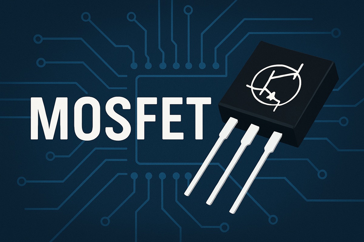
An entirely new model of the way electrons are briefly trapped and released in tiny electronic devices suggests that a long-accepted, industry-wide view is just plain wrong about the way these captured electrons affect the behavior of hardware components such as flash memory cells. The model which devised by scientists at the National Institute of Standards and Technology (abbreviation NIST),a measurement standards laboratory, and a non-regulatory agency of the United States Department of Commerce and its mission is to promote innovation and industrial competitiveness, was test to explain how electron capture and emission creates the insidious nosise that increasingly threatens performance as electronic devices continue to shrink in size.   KIN Cheung, NIST researcher Kin Cheung also the lead author of a new report in IEEE Transactions on Electron Devices said "Such a burst noise,popcorn noise or random telegraph noise(abbreviation RTN) have become a major problem for extremely small devicess". Charge trapping is one of the known causes of flash memory failure. The new model, which NIST physicist John Kramar called "a major paradigm shift in charge-trapping modeling," could lead to a different approach to manage this problem, and potentially, a new way of making the memory cells smaller. John Kramar explained:" Charge trapping is one of the known causes of flash memory failure,the new model whicl I called it a major paradigm shift in charge-trapping modeling,could lead to a different approach to manage this problem,and potentially,a new way of making the memory cells smaller.  What is RTN noise? RTN noise consists of abrupt random drops in voltage or current caused by itinerant electrons that are briefly captured from, and then rejoin, the main flow along a current channel in, for example, a common type of transistor called a MOSFET. "The effect was mostly negligible back in the good old days when devices were larger and there were lots of electrons flowing around," Cheung said. But in today's advanced devices, with feature dimensions in the range of 10 nanometers (nm, billionths of a meter) or less, the active area is so small that it can be swamped by a single trapped charge. "As you get down to the very smallest sizes, RTN can be nearly 100 percent as strong as the signal you're trying to measure," Cheung said. "In those conditions, reliability disappears." In the case of RTN, the basics are known: The noise is caused by the action of electrons near the interface between two materials such as an insulator layer and the bulk of the semiconductor in a transistor. Specifically, an electron is pulled out of the current flow and trapped in a defect in the insulator; after a short time, it is emitted back into the main current in the semiconductor. What actually happens on the atomic scale at each stage of the process, however, is incompletely understood. The orthodox approach to account for those effects is to treat all the trapped electrons as a single 2-D sheet of charge that extends uniformly across the center of the insulator. Each emitted electron is thought to return to the semiconductor in a reverse of the same process by which it was captured, causing very little change in the presumably stable state along the insulator/semiconductor boundary. The model is suitable for very small devices,however,it didn't make sense to the NIST scientists. Among other difficulties, it ignored the fact that, once they are immobilized, electrons cause considerable distortions in local electrical field conditions along the boundary, affecting current flow. "We're saying the traditional way doesn't really work," Cheung said. "You have to rethink this thing. The old model doesn't make reasonable assumptions about how charge carriers behave." The researchers proposed a new model, based on local effects, in which the mechanisms of capture and emission are dramatically different from the standard picture. For one thing, they determined that quantum mechanics, the modern theory that describes the behavior of these systems, makes it hugely improbable, if not impossible, for electrons to get out of the insulator the same way they got in. "It's like a highway where there is an exit ramp, but there's no on ramp," says NIST co-author Jason Campbell. "You can go in, but you can't come back that way. You've got to come back a different way. That is, there is a set of rules for capture that don't apply to emission." "When you realize that the capture and emission processes are decoupled," Cheung added, "you quickly have a very different view of the problem."  The standard RTN picture supposes a weak interaction of trapped charge with its local surroundings―in this case, the highly separated electric charge in the silicon dioxide that often makes up the insulator layer in a transistor. NIST scientists found that a weak interaction is inconsistent with known physics and not in agreement with reports from two independent laboratories. Indeed, the interaction energy of a captured electron can be more than 10 times greater than previously believed. Recognition of this stronger interaction energy enables the new local field picture to explain RTN naturally. The success of the new model, and the resulting drastic change in the understanding of both capture and emission, suggested that many long-held ideas would have to be thoroughly reconsidered. "It's a very scary and very unsetting conclusion,I mean,this is tear-up-the textbook stuff." Campbell said. As an end, NIST researchers hope the new model will help chip engineers and designers understand in much greater detail how devices degrade and hat will be required to get to the next stage of miniaturization while maintaining reliability and reducing noise. 
kynix On 2017-11-09   296
Memory

Use FeFETs to Build Memory,Futher Scaling,Simplified Processing and Power Consumption

As one of the world-leading research and innovation hub in nanoelectronics and digital technology,IMEC announced at the 2017 Symposia on VLSI Technology and Circuits that the world's first demonstration of a vertically stacked ferroelectric,AI doped HfO2 device for NAND applications.Using a new material and a novel architecture,imechas created a non-volatile memory concept with attractive characteristics for power consumption, switching speed, scalability and retention. The achievement shows that ferro-electric memory is a highly promising technology at various points in the memory hierarchy, and as a new technology for storage class memory. Imec will further develop the concept in collaboration with the world's leading producers of memory ICs.  Ferro-electric materials consist of crystals that exhibit spontaneous polarization; they can be in one of two states, which can be reversed with a suitable electric field. This non-volatile characteristic resembles ferromagnetism, after which they have been named. Discovered more than five decades ago, ferro-electric memory has always been considered ideal, due to its very low power needs, non-volatile character and high switching speed. However, issues with the complex materials, the breakdown of the interfacial layer and bad retention characteristics have presented significant challenges. The recent discovery of a ferro-electric phase in HfO2, a well-known and less complex material, has triggered a renewed interest in this memory concept.  "With HfO2, there is now a material with which we can process ferro-electric memories that are fully CMOS compatible. This allows us to make a ferro-electric FET (FeFET) in both planar and vertical varieties," noted Jan Van Houdt, imec's chief scientist for memory technology. "We are working to overcome some of the remaining issues, such as retention, precise doping techniques and interface properties, in order to stabilize the ferro-electric phase. We are now confident that our FeFET concept has all the required characteristics. It is, in fact, suitable for both stand-alone and embedded memories at various points in the memory hierarchy, going all the way from non-volatile DRAM to Flash-like memories. It has particularly interesting characteristics for future storage-class memory, which will help overcome the current bottleneck caused by the differences in speed between fast processors and slower mass memory." Imec recently presented the first, extremely positive results to its partners. The research center is now offering further development and industrialization of the vertical FeFET as a program to all its memory partners, which include the world's major companies producing memory ICs.  Van Houdt explained "FeFETs can be used as a technology to build memory very similar to Flash-memory, but with additional advantages for further scaling, simplified processing, and power consumption,with our longstanding R&D and processing experience on advanced Flash, we are uniquely positioned to offer our partners a head start in this exciting opportunity. They can then decide how best to fit ferro-electric memories in their products and chips." This is a breakthrough in CMOS-compatible ferroelectric memory, let's look forward to the CMOS-compatible ferroelectric memory together.  
kynix On 2017-11-01   413
Memory

Scientists Determine How Much Damage Memory Devices Can Take in Mass Transit Accidents

(Steve Cain is a senior research support specialist in the Integrated Electronics Engineering Center (IEEC) at Binghamton University. Credit: Jonathan Cohen/Binghamton University)While investigating mass transit accidents, especially in air travel, National Transportation Safety Board (NTSB) officials often rely on digital clues left behind in flash memories of any and all electronic devices—both personal and professional—at a crash site. With the physical forces and high-temperature fires associated with many crashes, memory units are often damaged and sometimes unreadable.Researchers at Binghamton University, State University of New York have figured out how much damage memory units can sustain before becoming unreadable and new repair techniques to retrieve clues off of damaged units, which might help prevent future tragedies."The biggest surprise was how much punishment these devices can take before ceasing to function," said Steve Cain, who is the project manager and a senior research support specialist in the Integrated Electronics Engineering Center (IEEC) at Binghamton University. "As part of their post-crash investigations, the NTSB collects anything and everything at the scene, including personal electronic devices. If the device was active during or just before the crash, it is possible that the data stored in the memory can provide clues as to the cause of the crash. Most of the time the device is ruined, but sometimes it is intact."The interdisciplinary Binghamton group of Cain, Preeth Sivakumar, Jack Lombardi, and Mark Poliks along with James Cash, Joseph Gregor, and Michael Budinski from the NTSB, presented "Fire Damage and Repair Techniques for Flash Memory Modules: Implication for Post-Crash Investigations" at the Fall 2016 International Symposium of Microelectronics.Scientists found plastic coverings started to break down after three hours of exposure to temperatures of 300 degrees Celsius, or about 572 degrees Fahrenheit or more, but memory chips were still readable.Researchers pointed out that even with the pressures and forces in play during past crashes, temperatures typically only reach those levels for short periods of time."Data integrity was maintained even in a plasma discharge," Cain said. "Basically, if the device doesn't burn up, there is a reasonable chance of the data being retained in the chip. The only problem is that the connections to the memory chips may be broken, so that the data cannot be read."For the second part of the study, researchers addressed the readability issue. The team purposely damaged memory units and then extracted memory chips using acid, lasers, plasma, or mechanical polishing.Lasers were the most effective extraction method and mechanical extractions was the simplest, but each method still damaged the wire bonds within memory chips and made many unreadable. A specialized metallic ink from a precision printer was used to restore functionality."These results expand the investigative scope for aviation accidents, where the data rather than the device is of paramount importance," the team concluded. "It is possible to repair the interconnections of flash memory modules, provided the chip is intact." Ref.AT27C1024-45JCEDD10161BBH-6ETS-F
kynix On 2017-07-28   275
Memory

Toshiba Memory Has Announced Development of The World’s First BiCS FLASH Three-dimensional (3D) Flash Memory

Toshiba Memory has announced development of the world’s first BiCS FLASH three-dimensional (3D) flash memory utilising Through Silicon Via (TSV) technology with 3-bit-per-cell (triple-level cell, TLC) technology. Shipments of prototypes for development purposes started in June, and product samples are scheduled for release in the second half of 2017. The prototype of this ground-breaking device will be showcased at the 2017 Flash Memory Summit in Santa Clara, California, United States, from August 7-10.Devices fabricated with TSV technology have vertical electrodes and vias that pass through silicon dies to provide connections, an architecture that realises high speed data input and output while reducing power consumption. Real-world performance has been proven previously, with the introduction of Toshiba’s 2D NAND Flash memory. Combining a 48-layer 3D flash process and TSV technology has allowed Toshiba Memory Corporation to successfully increase product programming bandwidth while achieving low power consumption. The power efficiency of a single package is approximately twice that of the same generation BiCS FLASH memory fabricated with wire-bonding technology. TSV BiCS FLASH also enables a 1-terabyte (TB) device with a 16-die stacked architecture in a single package. Toshiba Memory will commercialise BiCS FLASH with TSV technology to provide an ideal solution in respect for storage applications requiring low latency, high bandwidth and high IOPS/W, including high-end enterprise SSDs. Ref.KY32-CG7937AAKY32-CG7797AAT
kynix On 2017-07-21   271
Memory

A better data storage in the making

Techniques and coding theories in information sciences have helped to design new concepts for faster and better data storage. Rapid and reliable data storage is crucial for the success of businesses, online platforms, information repositories and research centres. The EU-funded INFO-STORE (Novel data storage by advancing information sciences) project investigated how to overcome challenges and limitations in emerging data storage applications.Combining theory, practice and expert discussions in a series of five subprojects, the project examined how to improve information storage through breakthroughs in coding theory and related theoretical disciplines. The project made significant progress with respect to multilevel non-volatile memories and their trade-offs between storage density and read/write speeds. This included designing new coding frameworks to improve read/write speeds, maximising the number of writes, reading memory cells in parallel, and balancing density and speed in multilevel memories. To develop high-throughput memory systems for network switches and routers, INFO-STORE produced a coding framework that switches packets between input and output ports. This also involved new codes for optimal switching guarantees, algorithms that exploit such codes in a network switch or router, and compression of forwarding databases. The achievements in this vein overcame the challenge of memory contention in network switches and routers. High-density memristor (resistive memory) storage and associated reliability challenges were also studied to avoid a key obstacle known as sneak paths. In addition, work on memristor issues involved using regular arrays of memristor devices that combine storage and logic. Another important project milestone involved distributed storage systems and the need for flexible data reconstruction in the presence of failing and busy nodes. To overcome this obstacle, INFO-STORE developed a 2D coding framework that allows only a number of nodes to provide a small portion of their stored information – i.e. partial delivery. Lastly, researchers proposed efficient data distribution schemes that work well with the short packet blocks. As data distribution schemes using fountain codes operate optimally only when the packet blocks are very large, the team produced a coding scheme to optimise encoder operation for the receiver's state. This lowers the overhead considerably for short blocks. The project's results were followed by many other ideas and proposals, including a publication on elastic compression of content in web servers to improve server security against denial-of-service attacks. The project's research findings have already begun contributing to the development of quicker, better and safer data storage. Ref.KY32-CY7C1357S-100AXCKY32-CY7C131E-55NXI
kynix On 2017-07-12   322
Memory

Breakthrough in CMOS-compatible ferroelectric memory

Imec, the world-leading research and innovation hub in nanoelectronics and digital technology, announced today at the 2017 Symposia on VLSI Technology and Circuits the world's first demonstration of a vertically stacked ferroelectric Al doped HfO2 device for NAND applications. Using a new material and a novel architecture, imec has created a non-volatile memory concept with attractive characteristics for power consumption, switching speed, scalability and retention. The achievement shows that ferro-electric memory is a highly promising technology at various points in the memory hierarchy, and as a new technology for storage class memory. Imec will further develop the concept in collaboration with the world's leading producers of memory ICs.  Ferro-electric materials consist of crystals that exhibit spontaneous polarization; they can be in one of two states, which can be reversed with a suitable electric field. This non-volatile characteristic resembles ferromagnetism, after which they have been named. Discovered more than five decades ago, ferro-electric memory has always been considered ideal, due to its very low power needs, non-volatile character and high switching speed. However, issues with the complex materials, the breakdown of the interfacial layer and bad retention characteristics have presented significant challenges. The recent discovery of a ferro-electric phase in HfO2, a well-known and less complex material, has triggered a renewed interest in this memory concept."With HfO2, there is now a material with which we can process ferro-electric memories that are fully CMOS compatible. This allows us to make a ferro-electric FET (FeFET) in both planar and vertical varieties," noted Jan Van Houdt, imec's chief scientist for memory technology. "We are working to overcome some of the remaining issues, such as retention, precise doping techniques and interface properties, in order to stabilize the ferro-electric phase. We are now confident that our FeFET concept has all the required characteristics. It is, in fact, suitable for both stand-alone and embedded memories at various points in the memory hierarchy, going all the way from non-volatile DRAM to Flash-like memories. It has particularly interesting characteristics for future storage-class memory, which will help overcome the current bottleneck caused by the differences in speed between fast processors and slower mass memory."Imec recently presented the first, extremely positive results to its partners. The research center is now offering further development and industrialization of the vertical FeFET as a program to all its memory partners, which include the world's major companies producing memory ICs."FeFETs can be used as a technology to build memory very similar to Flash-memory, but with additional advantages for further scaling, simplified processing, and power consumption," added Van Houdt. "With our longstanding R&D and processing experience on advanced Flash, we are uniquely positioned to offer our partners a head start in this exciting opportunity. They can then decide how best to fit ferro-electric memories in their products and chips." Ref:KY32-K9T1G08U0M-YIBOKY32-CY7C1357S-100AXCKY32-AT49BV162AT(T)  
kynix On 2017-06-10   416

Kynix

Kynix was founded in 2008, specializing in the electronic components distribution business. We adhere to honesty and ethics as our business philosophy and have gradually established an excellent reputation and credibility in our international business. With the accurate quotation, excellent credit, reasonable price, reliable quality, fast delivery, and authentic service, we have won the praise of the majority of customers.

Follow us

Join our mailing list!

Be the first to know about new products, special offers, and more.

Kynix

  • How to purchase

  • Order
  • Search & Inquiry
  • Shipping & Tracking
  • Payment Methods
  • Contact Us

  • Tel: 00852-6915 1330
  • Email: info@kynix.com
  • Follow Us

authentication

Kynix

© 2008-2026 kynix.com all rights reserve.