info@kynix.com
 00852-6915 1330


 0
0



.jpg "structure and electrical symbol (depletion mode mosfet)")


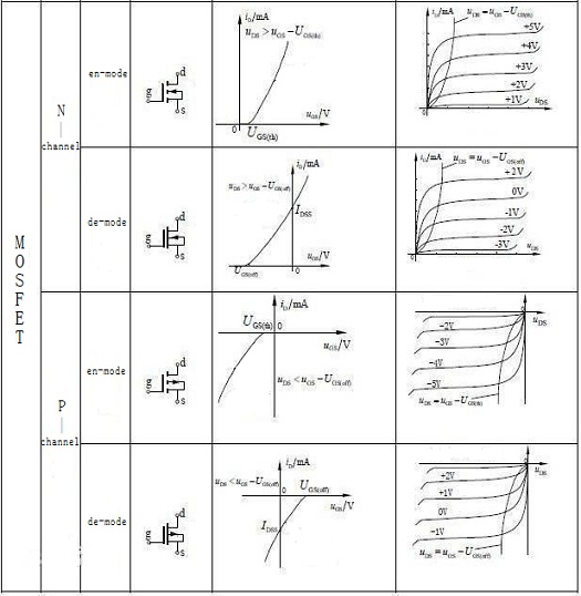
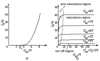
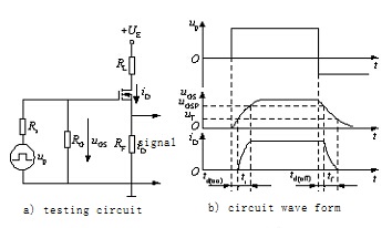
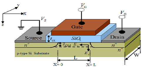


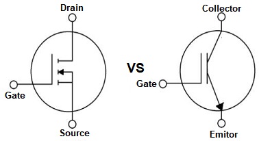
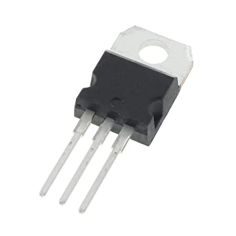
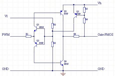
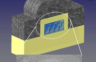
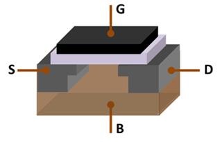
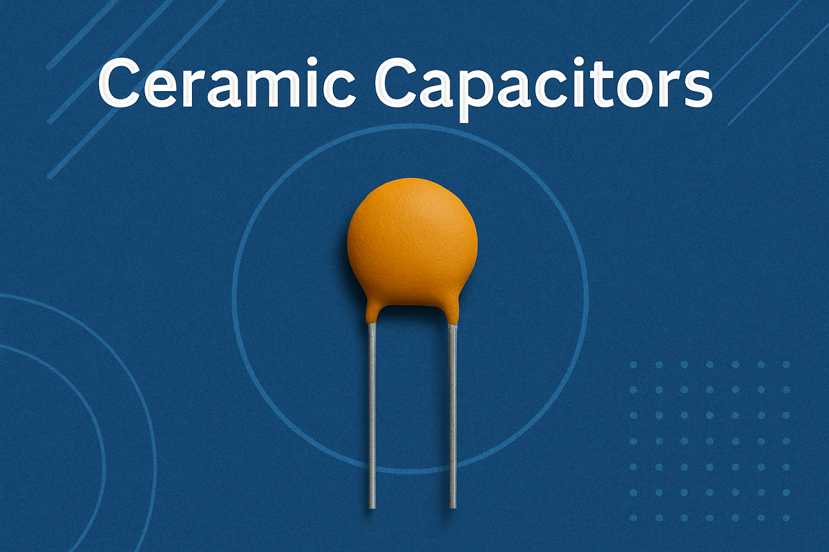
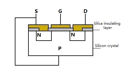
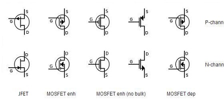
1. Introduction to MOSFETs In the world of modern electronics, few components have revolutionized circuit design as profoundly as the Metal-Oxide-Semiconductor Field-Effect Transistor (MOSFET). These tiny yet powerful semiconductor devices have become the backbone of contemporary electronic systems, from smartphones and laptops to industrial equipment and automotive electronics. Figure 1: Various types of MOSFET packages used in modern electronics Did you know that a single advanced microprocessor can contain billions of MOSFETs on a chip smaller than your fingernail? This incredible density has enabled the computing revolution we take for granted today. MOSFETs have become fundamental building blocks for both analog and digital circuits due to their unique electrical properties and outstanding performance. The MOSFET differs significantly from its predecessor, the bipolar junction transistor (BJT), by operating as a voltage-controlled device rather than a current-controlled one. This fundamental difference makes MOSFETs exceptionally energy-efficient and ideal for applications where power consumption is a critical concern. "MOSFETs represent one of the most significant technological breakthroughs in semiconductor history, enabling the dramatic miniaturization and increased efficiency of electronic devices over the past five decades." In this comprehensive guide, we'll explore the working principles, types, applications, and selection criteria for MOSFETs. Whether you're an electronics enthusiast, engineering student, or professional designer, understanding these versatile components will enhance your ability to create efficient and innovative electronic systems. 2. MOSFET Working Principles 2.1 Basic Structure and Components At its core, a MOSFET consists of several key components working together to control electrical current flow. Understanding the physical structure of a MOSFET is essential to grasp its operating principles and capabilities. Figure 2: Basic structure of a MOSFET showing key components The fundamental components of a MOSFET include: Gate Terminal: The control electrode that regulates current flow through the device. It's separated from the semiconductor material by an insulating oxide layer.Source Terminal: The terminal where charge carriers enter the device.Drain Terminal: The terminal where charge carriers exit the device.Substrate (Body): The semiconductor material that forms the foundation of the device, typically made of silicon.Oxide Layer: A thin insulating layer (usually silicon dioxide) that separates the gate from the channel, preventing direct electrical contact.Channel: The region between source and drain where current flows when the device is turned on. The name MOSFET itself describes its construction: Metal (gate electrode), Oxide (insulating layer), and Semiconductor (substrate), combined with Field-Effect Transistor (operating principle). Pro Tip: MOSFETs are sometimes called IGFETs (Insulated Gate Field-Effect Transistors) because the gate is electrically insulated from the channel, which is a key feature distinguishing them from other transistor types. 2.2 Operation Modes MOSFETs operate in different modes depending on the voltage applied to their terminals. The two primary modes are enhancement mode and depletion mode. Enhancement Mode Figure 3: Enhancement Mode MOSFET operation In enhancement mode operation: The MOSFET acts like an open switch when no voltage is applied to the gate (normally OFF).A conductive channel forms between source and drain only when sufficient voltage is applied to the gate.For N-channel enhancement MOSFETs, a positive gate voltage is required to create an electron-rich channel.For P-channel enhancement MOSFETs, a negative gate voltage is required to create a hole-rich channel. Depletion Mode Figure 4: Depletion Mode MOSFET operation In depletion mode operation: The MOSFET has a conductive channel even with no gate voltage (normally ON).Applying a voltage of appropriate polarity to the gate reduces or "depletes" the channel, decreasing current flow.For N-channel depletion MOSFETs, a negative gate voltage depletes the channel.For P-channel depletion MOSFETs, a positive gate voltage depletes the channel. MOSFETs also operate in three distinct regions based on the relationship between gate-source voltage (VGS) and drain-source voltage (VDS): Cut-off Region: The MOSFET is turned off, and no significant current flows between drain and source.Ohmic (Linear) Region: The MOSFET acts like a voltage-controlled resistor, with current proportional to voltage.Saturation Region: The MOSFET delivers a relatively constant current regardless of increases in drain-source voltage. 2.3 Electrical Characteristics MOSFETs exhibit several important electrical characteristics that determine their performance in circuits: Threshold Voltage (Vth) The threshold voltage is the minimum gate-source voltage required to create a conductive channel between source and drain. Typical threshold values range from 1-4V, with lower voltages (1-2V) for logic-level MOSFETs designed to work with digital circuits, and higher voltages for power applications. On-Resistance (RDS(on)) On-resistance is the resistance between drain and source when the MOSFET is fully turned on. Lower RDS(on) values result in less power dissipation and higher efficiency. Modern power MOSFETs can achieve RDS(on) values below 1 milliohm for high-current applications. Transconductance (gm) Transconductance measures how efficiently the gate voltage controls the drain current. Higher transconductance values indicate better control and amplification capabilities. Gate Charge (Qg) Gate charge represents the amount of electrical charge required to turn the MOSFET on. Lower gate charge values enable faster switching speeds and lower switching losses, which is critical in high-frequency applications. Breakdown Voltage (VDSS or BVDSS) This is the maximum voltage the MOSFET can withstand between drain and source before breakdown occurs. Power MOSFETs are available with breakdown voltages ranging from tens to thousands of volts. Important Note: The relationship between on-resistance and breakdown voltage involves a fundamental tradeoff in MOSFET design. Higher breakdown voltage ratings generally result in higher on-resistance, which means increased power losses during conduction. This tradeoff must be carefully considered when selecting MOSFETs for specific applications. 3. Types of MOSFETs 3.1 N-Channel vs P-Channel Figure 5: Comparison of N-Channel and P-Channel MOSFETs MOSFETs are primarily classified by the type of charge carriers that form their conductive channel: N-Channel MOSFETs In N-channel MOSFETs, electrons serve as the primary charge carriers. These MOSFETs: Turn on with a positive gate voltage relative to the sourceOffer higher electron mobility, resulting in lower on-resistance and better efficiencyAre more commonly used due to superior performance characteristicsTypically serve as "low-side switches" where the load is connected between the positive supply and the drain P-Channel MOSFETs In P-channel MOSFETs, holes (absence of electrons) serve as the primary charge carriers. These MOSFETs: Turn on with a negative gate voltage relative to the sourceHave higher on-resistance than equivalent N-channel devices (typically 2-3 times higher)Are often used as "high-side switches" where the load is connected between the drain and groundSimplify circuit design in certain applications despite lower efficiencyCharacteristicN-Channel MOSFETP-Channel MOSFETCharge CarriersElectronsHolesGate Voltage to Turn OnPositive relative to sourceNegative relative to sourceTypical ApplicationLow-side switchingHigh-side switchingEfficiencyHigher (lower RDS(on))Lower (higher RDS(on))Circuit Symbol DirectionArrow pointing outwardArrow pointing inward 3.2 Enhancement vs Depletion Mode Figure 6: Enhancement and Depletion Mode MOSFETs Beyond the channel type, MOSFETs are further classified based on their default state without applied gate voltage: Enhancement Mode MOSFETs Enhancement mode MOSFETs are normally OFF when no voltage is applied to the gate. They require an appropriate gate voltage to enhance (create) a conductive channel. Enhancement mode devices are the most common MOSFETs in modern electronics because: They consume no power when off (ideal for battery-powered devices)They offer simplified circuit protection in failure scenariosThey provide more predictable operation in most digital and power circuits Depletion Mode MOSFETs Depletion mode MOSFETs are normally ON when no voltage is applied to the gate. They require an appropriate gate voltage to deplete (remove) the existing conductive channel. Although less common, they offer advantages in: Certain analog circuits where a normally-on condition is desirableApplications requiring fail-safe operation when gate drive is lostSpecific circuit topologies like cascode configurationsPro Tip: Enhancement mode MOSFETs are often symbolized with a broken channel line in circuit diagrams, while depletion mode MOSFETs are shown with a solid channel line. This visual difference helps engineers quickly identify the device type in schematics. 3.3 Power MOSFETs Power MOSFETs are specialized versions designed to handle higher voltages and currents. They feature several important design variations: Figure 7: Various power MOSFET package types Vertical MOSFETs Most power MOSFETs use a vertical structure where current flows from the drain at the bottom of the chip to the source at the top. This design maximizes current handling capability and voltage blocking ability. Planar vs. Trench Technology Power MOSFETs are manufactured using either planar or trench technology: Planar MOSFETs: The older technology with the gate and channel formed on the surface of the siliconTrench MOSFETs: A newer design where the gate structure extends into trenches etched into the silicon, providing higher cell density and lower on-resistance Packaging Options Power MOSFETs come in various package types based on thermal and current requirements: Through-hole packages (TO-220, TO-247): Offer excellent thermal performance and easy mountingSurface-mount packages (DPAK, D2PAK, SO-8): Provide space efficiency for automated assemblyPQFN packages: Offer ultra-low profile and excellent thermal performanceDirectFET packages: Provide optimized thermal and electrical performance for high-efficiency applications"The development of power MOSFETs has been one of the key enablers for the miniaturization of power electronics, allowing engineers to create smaller, more efficient power supplies and motor drives than ever before possible." 4. Applications of MOSFETs Figure 8: Common applications of MOSFETs in modern electronics MOSFETs are among the most versatile semiconductor devices, finding applications across virtually every sector of electronics. Their unique properties make them ideal for a wide range of functions, from simple switching to complex signal processing. 4.1 Switching Applications One of the most common uses of MOSFETs is as electronic switches. Their ability to transition quickly between high-resistance (off) and low-resistance (on) states makes them ideal for controlling power to various loads. Low-Side and High-Side Switching MOSFETs can be configured as: Low-side switches: N-channel MOSFETs placed between the load and groundHigh-side switches: P-channel MOSFETs or specially driven N-channel MOSFETs placed between the power supply and the load Pulse Width Modulation (PWM) MOSFETs excel in PWM applications where rapid switching is required to control: 4.2 Amplification Applications MOSFETs serve as excellent amplifiers due to their high input impedance and good frequency response. They are used in: The extremely high input impedance of MOSFETs (typically 1010 to 1015 ohms) allows them to amplify signals without loading down the source, making them ideal for applications where minimal signal distortion is critical. 4.3 Integrated Circuits MOSFETs form the foundation of modern integrated circuit technology: Digital Logic CMOS (Complementary MOS) technology, which combines N-channel and P-channel MOSFETs, dominates digital logic implementation due to its: Low power consumption during static operationHigh noise immunityWide operating voltage rangeHigh integration density Memory MOSFETs are essential in various memory technologies: DRAM (Dynamic RAM): Uses MOSFETs as access transistors for storage capacitorsSRAM (Static RAM): Uses multiple MOSFETs to form bistable latchesFlash memory: Uses specially designed floating-gate MOSFETs to store charge Microprocessors Modern CPUs and microcontrollers contain billions of MOSFETs, with each one serving as a fundamental switching element in the processor's logic circuits. Pro Tip: The miniaturization of MOSFETs following Moore's Law has been the driving force behind the exponential increase in computing power over the past several decades. Today's most advanced processes can create MOSFETs with features as small as 5 nanometers. 4.4 Power Electronics Applications Power MOSFETs handle substantial current and voltage levels in various applications: Power Supplies MOSFETs are critical components in modern switching power supplies: DC-DC converters: Buck, boost, and buck-boost topologiesAC-DC power supplies: Power factor correction stages and synchronous rectificationUninterruptible power supplies (UPS): Inverter stages and battery management Motor Control MOSFETs provide precise control in various motor drive applications: Brushless DC motor controllers in drones and electric vehiclesVariable frequency drives for industrial motorsStepper motor drivers in 3D printers and CNC machinesServo controllers in robotics and automation Automotive Electronics Modern vehicles use MOSFETs extensively in: Electronic control units (ECUs)LED lighting systemsBattery management systemsElectric power steeringElectric and hybrid vehicle powertrains The automotive industry has driven significant advancements in MOSFET technology, demanding devices that can operate reliably in harsh environments with extreme temperature variations and strict reliability requirements. 5. How to Select the Right MOSFET Choosing the appropriate MOSFET for a specific application requires careful consideration of various parameters and requirements. This section provides a structured approach to MOSFET selection based on application needs. 5.1 Key Parameters to Consider Voltage Ratings When selecting a MOSFET, voltage ratings are among the most critical specifications to consider: VDSS (Drain-Source Breakdown Voltage): Should be at least 20-50% higher than the maximum voltage the MOSFET will experience in the circuitVGS(max) (Maximum Gate-Source Voltage): Defines the maximum allowable gate drive voltageVGS(th) (Gate Threshold Voltage): Must be compatible with your gate driver capability Current Ratings Current handling capability determines whether the MOSFET can safely operate in your application: ID (Continuous Drain Current): Should exceed the maximum continuous current required by your application with a safety margin of at least 50%IDM (Pulsed Drain Current): Important for applications with periodic current surgesSafe Operating Area (SOA): Defines the safe combinations of voltage, current, and time duration Resistance and Power Dissipation These parameters affect efficiency and thermal management: RDS(on) (Drain-Source On-Resistance): Lower values mean less power dissipation and higher efficiencyPD (Maximum Power Dissipation): Must exceed the calculated power dissipation in your applicationRθJC (Thermal Resistance, Junction-to-Case): Lower values indicate better heat transfer capability Switching Parameters For applications involving frequent switching, these parameters are crucial: Qg (Total Gate Charge): Lower values enable faster switching and reduce drive requirementstr and tf (Rise and Fall Times): Determine how quickly the MOSFET can transition between on and off statesCiss, Coss, Crss (Input, Output, and Reverse Transfer Capacitances): Affect switching behavior and frequency responseParameterSymbolImportanceTypical RangeDrain-Source Breakdown VoltageVDSSCritical for preventing breakdown20V to 1500V+Continuous Drain CurrentIDDetermines current handling capability1A to 300A+On-ResistanceRDS(on)Critical for efficiency0.5mΩ to 100ΩGate Threshold VoltageVGS(th)Must match drive capability1V to 4VTotal Gate ChargeQgImportant for switching speed1nC to 300nC 5.2 Application Requirements Analysis Different applications place different demands on MOSFETs. Here's how to match MOSFET characteristics to application requirements: Switching Applications For applications where the MOSFET primarily functions as a switch: Prioritize low RDS(on) to minimize conduction lossesConsider gate charge (Qg) for high-frequency switchingEnsure adequate voltage margin (VDSS) to prevent breakdownChoose logic-level gate threshold if driving from microcontrollers or low-voltage logic Amplifier Applications For linear operation in amplifiers: Focus on transconductance (gm) for better gainConsider noise characteristics, especially in audio applicationsLook for devices with good linearity in their transfer characteristicsSelect devices with appropriate frequency response for the signal bandwidth Power Management Applications For power conversion and management: 5.3 Thermal Considerations Thermal management is critical for MOSFET reliability and performance: Power Dissipation Calculation Calculate power dissipation considering both conduction and switching losses: Conduction losses: Pcond = ID2 × RDS(on)Switching losses: Psw = f × Esw (where f is frequency and Esw is energy loss per switching cycle)Total losses: Ptotal = Pcond + Psw Thermal Resistance Understand the thermal path from junction to ambient: RθJC (Junction to Case): Inherent to the MOSFET packageRθCS (Case to Heatsink): Depends on mounting method and thermal interface materialRθSA (Heatsink to Ambient): Depends on heatsink design and airflow Temperature Rise Calculation Calculate junction temperature using: Tj = Ta + Ptotal × (RθJC + RθCS + RθSA) Where Tj is junction temperature and Ta is ambient temperature. Important Note: Always ensure that the calculated junction temperature remains well below the maximum rated junction temperature (typically 150°C to 175°C) with adequate margin for reliability. A good practice is to design for maximum junction temperatures no higher than 110-120°C for long-term reliability. 6. Advantages and Disadvantages 6.1 Benefits of MOSFETs Advantages of MOSFETs High Input Impedance: Virtually no gate current required for operation, minimizing power requirements for control circuitsFast Switching Speed: Capable of operating at frequencies from kilohertz to gigahertz, making them suitable for high-frequency applicationsLow Power Consumption: Minimal power required in the OFF state and low power losses in modern designsPositive Temperature Coefficient: Resistance increases with temperature, allowing easy parallel connection without thermal runawayNo Second Breakdown: More robust against thermal overload compared to bipolar transistorsVoltage-Controlled Device: Simple drive requirements with minimal control powerThermal Stability: Better performance at high temperatures compared to BJTsEasy Paralleling: Multiple devices can be connected in parallel to increase current handling These advantages have made MOSFETs the dominant technology in many applications, especially those requiring high efficiency, fast switching, or minimal control power. 6.2 Limitations of MOSFETs Disadvantages of MOSFETs ESD Sensitivity: The thin gate oxide makes MOSFETs susceptible to damage from electrostatic dischargeGate Drive Requirements: Some MOSFETs require specific voltage levels for proper operationHigher Cost: Can be more expensive than BJTs in certain applicationsOn-Resistance Increases with Voltage Rating: Higher voltage MOSFETs have higher RDS(on), leading to lower efficiencyBody Diode Limitations: The intrinsic body diode may have poor reverse recovery characteristicsMiller Effect: Capacitive feedback can cause unwanted oscillations and switching issuesThermal Runaway in Linear Applications: When operating in the linear region, MOSFETs can suffer from thermal instability Understanding these limitations is crucial for designing reliable circuits. Proper MOSFET selection and circuit design can mitigate many of these disadvantages. 6.3 MOSFETs vs BJTs Bipolar Junction Transistors (BJTs) and MOSFETs are both transistors, but they operate on different principles and have distinct characteristics: CharacteristicMOSFETBJTControl ParameterVoltage-controlled (gate voltage)Current-controlled (base current)Input ImpedanceVery high (1010-1015 Ω)Moderate (1-10 kΩ)Switching SpeedVery fastModerateThermal StabilityGood (positive temperature coefficient)Poor (negative temperature coefficient)Ease of ParallelingExcellentPoorOn-State Voltage DropHigher at high voltages (>200V)Lower at high voltagesESD SensitivityHighLow The choice between MOSFETs and BJTs depends on application requirements: MOSFETs excel in: High-frequency switching, low power applications, parallel operation, digital circuitsBJTs excel in: High-voltage linear amplifiers, cost-sensitive applications with moderate switching speeds, circuits needing low on-state voltage drop 6.4 MOSFETs vs IGBTs Insulated Gate Bipolar Transistors (IGBTs) combine features of both MOSFETs and BJTs: CharacteristicMOSFETIGBTVoltage RangeBetter for <250V applicationsBetter for >600V applicationsSwitching SpeedFaster (nanoseconds to microseconds)Slower (microseconds)On-State Voltage DropResistive (I×RDS(on))Fixed voltage drop + small resistive componentCurrent DensityLowerHigherConduction Losses at High VoltageHigherLowerSwitching LossesLowerHigherParallelingEasyMore difficult Application guidelines for choosing between MOSFETs and IGBTs: Choose MOSFETs for: Lower voltage applications (<600V), high-frequency switching (>20kHz), lower current requirementsChoose IGBTs for: Higher voltage applications (>1000V), lower frequency operation (<20kHz), higher current requirementsConsider both in: The 600-1000V range, where the choice depends on specific requirements for switching speed versus conduction lossesPro Tip: In the midrange (600-1000V) at moderate currents, the latest generations of wide bandgap semiconductors like Silicon Carbide (SiC) MOSFETs are challenging IGBTs by offering both low conduction losses and fast switching speeds, though at a premium price. 7. Latest Advancements in MOSFET Technology The field of MOSFET technology continues to evolve rapidly, with several significant innovations expanding their capabilities and applications: Wide Bandgap Semiconductors Silicon Carbide (SiC) MOSFETs and Gallium Nitride (GaN) MOSFETs represent major advancements over traditional silicon devices: Higher breakdown voltage capabilities (up to 1700V for commercial SiC devices)Lower on-resistance for a given voltage ratingFaster switching speeds with reduced lossesBetter thermal conductivity allowing operation at higher temperaturesSmaller die size for the same power handling capability These wide bandgap devices are enabling more efficient power conversion in electric vehicles, solar inverters, and industrial motor drives, with efficiency improvements of 2-5% compared to silicon-based solutions. Superjunction Technology Superjunction MOSFETs use a unique charge-balanced structure to overcome the traditional silicon MOSFET limitations: Dramatically reduced RDS(on) for a given breakdown voltageBetter figure of merit (RDS(on) × gate charge) for improved efficiencyEnhanced switching performance in the 500-900V rangeImproved ruggedness and reliability in hard-switching applications Advanced Packaging Technologies Innovations in MOSFET packaging are addressing thermal and parasitic challenges: Clip-bond technology: Replaces traditional wire bonds with metal clips for lower resistance and inductanceDouble-sided cooling: Allows heat extraction from both sides of the dieCopper clip technology: Improves current handling and thermal performanceIntegrated packages: Combining multiple MOSFETs or drivers with MOSFETs in a single package Specialized MOSFET Types New MOSFET designs address specific application challenges: Radiation-hardened MOSFETs: For space and nuclear applicationsUltra-low RDS(on) MOSFETs: For battery-powered and automotive applicationsFast-recovery body diode MOSFETs: For synchronous rectification applicationsIntegrated protection features: MOSFETs with built-in temperature, current, and voltage protection"The development of wide bandgap semiconductors represents the most significant advancement in power MOSFET technology in the past two decades, enabling power conversion efficiency levels that were previously unattainable with silicon devices." 8. Frequently Asked Questions Q1: How can I test if a MOSFET is working properly? To test a MOSFET's functionality, you can use a digital multimeter with diode test mode. For N-channel MOSFETs: For P-channel MOSFETs, reverse the probe polarities in the above procedure. Q2: What's the difference between a logic-level and standard MOSFET? Logic-level MOSFETs are designed to be fully turned on at lower gate voltages (typically 3.3-5V) compatible with digital logic outputs. Standard MOSFETs generally require higher gate voltages (8-10V or more) to achieve their rated performance. The key differences include: Logic-level MOSFETs have a lower threshold voltage (VGS(th)), usually below 2VThey achieve their specified RDS(on) at gate voltages of 4.5-5VThey're ideal for microcontroller-driven applicationsHowever, they typically have higher RDS(on) than standard MOSFETs of the same size when both are fully enhancedQ3: Why do MOSFETs get hot, and how can I prevent this? MOSFETs generate heat primarily due to three factors: Conduction losses: I2R losses from current flowing through RDS(on)Switching losses: Energy lost during transitions between on and off statesLinear operation losses: High power dissipation when operating in the linear region To prevent overheating: Select MOSFETs with lower RDS(on) for high-current applicationsUse appropriate heatsinking and thermal designAvoid operating MOSFETs in the linear region for extended periodsOptimize gate drive for faster switching transitionsUse snubber circuits to minimize switching lossesConsider parallel MOSFETs to distribute current and heatQ4: Can I use N-channel and P-channel MOSFETs interchangeably? N-channel and P-channel MOSFETs cannot be used interchangeably without circuit modifications, as they: Respond to opposite gate voltage polaritiesHave current flowing in different directionsTypically have different performance characteristics (N-channel usually has lower RDS(on)) When replacing one with the other, you'll need to: Invert the gate drive signalReconfigure the circuit topologyAdjust component values to accommodate different characteristicsConsider that N-channel devices are typically more efficient for low-side switching, while P-channel devices simplify high-side switching in some applicationsQ5: What causes MOSFET failure, and how can I protect against it? Common causes of MOSFET failure include: Overvoltage: Exceeding the maximum drain-source or gate-source voltage ratingsOvercurrent: Exceeding safe current limits or operating outside the Safe Operating Area (SOA)Overtemperature: Operating beyond the maximum junction temperaturedv/dt failure: Excessive voltage change rates triggering parasitic structuresESD damage: Electrostatic discharge damaging the gate oxideGate oxide breakdown: Excessive gate voltage stressing the thin oxide layer Protection strategies include: 9. Conclusion and Future Outlook MOSFETs have transformed electronics since their introduction, enabling the miniaturization, efficiency improvements, and performance enhancements that define modern electronic systems. From tiny signal-level applications to high-power industrial drives, these versatile components continue to evolve and expand their capabilities. The key strengths of MOSFETs include: Exceptional switching performance and efficiencyHigh input impedance and minimal drive requirementsWide range of available specifications to suit diverse applicationsContinuing technological advances expanding their capabilitiesExcellent integration capability in both discrete and IC forms Looking ahead, several trends will shape the future of MOSFET technology: Wide Bandgap Adoption: SiC and GaN MOSFETs will continue to penetrate high-performance power applications, offering unprecedented efficiency in electric vehicles, renewable energy systems, and industrial drives.Integration: More integrated solutions combining MOSFETs with drivers, protection, and control circuitry will simplify design and improve reliability.Miniaturization: Continued advancements in manufacturing will enable smaller MOSFETs with improved performance, supporting the trend toward more compact electronic devices.Specialization: Application-specific MOSFETs tailored for particular use cases will proliferate, with optimizations for automotive, renewable energy, data centers, and consumer electronics.Intelligent Power Devices: MOSFETs with embedded sensing and protection features will enable smarter power systems with enhanced reliability and diagnostic capabilities. Understanding MOSFET technology is increasingly valuable for anyone working in electronics, from hobbyists and students to professional engineers. By mastering the principles, types, and selection criteria presented in this guide, you'll be well-equipped to harness the full potential of these remarkable devices in your own projects and designs. Final Recommendation: When working with MOSFETs, always refer to manufacturer datasheets for specific parameters and recommended operating conditions. Begin your design process by clearly defining your application requirements, then select MOSFETs that provide adequate performance margins for voltage, current, and thermal considerations to ensure reliability under all operating conditions. Further Reading Difference and Relation Between IGBTs and MOSFETsThe Best Tutorial for P-Channel MOSFET External Resources MOSFET - WikipediaList of MOSFET Applications - WikipediaMOSFET Types, Working, Structure, and Applications - ElectronicsForuPower MOSFET Basics - Infineon TechnologiesLast Updated: May 2025 body { font-family: 'Segoe UI', Tahoma, Geneva, Verdana, sans-serif; line-height: 1.6; color: #333; background-color: #f9fafb; } .container { max-width: 1200px; margin: 0 auto; padding: 20px; } h1, h2, h3, h4, h5 { font-weight: 700; margin-top: 1.5em; margin-bottom: 0.75em; color: #2563eb; } h1 { font-size: 2.5rem; margin-top: 0.5em; color: #1e40af; } h2 { font-size: 2rem; border-bottom: 2px solid #ddd; padding-bottom: 0.3em; } h3 { font-size: 1.5rem; color: #3b82f6; } p { margin-bottom: 1.2em; font-size: 1.1rem; } .quote-block { background-color: #e0f2fe; border-left: 4px solid #3b82f6; padding: 15px; margin: 20px 0; font-style: italic; } .pro-tip { background-color: #d1fae5; border-left: 4px solid #059669; padding: 15px; margin: 20px 0; } .important-note { background-color: #fee2e2; border-left: 4px solid #ef4444; padding: 15px; margin: 20px 0; } .image-container { margin: 20px 0; text-align: center; } .image-container img { max-width: 100%; height: auto; border-radius: 5px; box-shadow: 0 4px 6px -1px rgba(0, 0, 0, 0.1), 0 2px 4px -1px rgba(0, 0, 0, 0.06); } .image-caption { text-align: center; font-style: italic; color: #6b7280; margin-top: 8px; } table { width: 100%; border-collapse: collapse; margin: 20px 0; } th, td { border: 1px solid #ddd; padding: 12px; text-align: left; } th { background-color: #2563eb; color: white; } tr:nth-child(even) { background-color: #f2f2f2; } .table-container { overflow-x: auto; margin: 20px 0; } .toc { background-color: #f1f5f9; border-radius: 5px; padding: 20px; margin: 20px 0; } .toc-title { font-size: 1.5rem; margin-bottom: 15px; color: #1e40af; } .toc ol { list-style-type: decimal; margin-left: 20px; } .toc ol ol { list-style-type: lower-alpha; margin-left: 25px; } .toc li { margin-bottom: 8px; } .toc a { color: #2563eb; text-decoration: none; } .toc a:hover { text-decoration: underline; } .external-link { color: #2563eb; text-decoration: none; font-weight: bold; border-bottom: 1px dotted #2563eb; } .external-link:hover { color: #1e40af; } .internal-link { color: #059669; text-decoration: none; font-weight: bold; border-bottom: 1px dotted #059669; } .internal-link:hover { color: #047857; } .rating { display: flex; align-items: center; margin: 20px 0; } .star { color: #fbbf24; font-size: 1.5rem; margin-right: 3px; } .author-info { display: flex; align-items: center; margin-top: 30px; margin-bottom: 30px; background-color: #f1f5f9; padding: 15px; border-radius: 5px; } .author-avatar { width: 60px; height: 60px; border-radius: 50%; margin-right: 15px; } .last-updated { font-style: italic; color: #6b7280; margin-top: 40px; } .faq-item { margin-bottom: 20px; } .faq-question { font-weight: 700; color: #1e40af; margin-bottom: 10px; } .highlight { background-color: #fef3c7; padding: 0 3px; border-radius: 3px; } .pros-cons-container { display: flex; flex-wrap: wrap; gap: 20px; margin: 20px 0; } .pros-container, .cons-container { flex: 1; min-width: 300px; border-radius: 5px; padding: 20px; } .pros-container { background-color: #f0fdf4; border: 1px solid #86efac; } .cons-container { background-color: #fef2f2; border: 1px solid #fecaca; } .pros-cons-title { font-weight: 700; margin-bottom: 15px; color: #333; font-size: 1.2rem; } .pros-cons-list { list-style-type: none; padding-left: 10px; } .pros-cons-list li { margin-bottom: 8px; position: relative; padding-left: 25px; } .pros-cons-list li:before { position: absolute; left: 0; font-family: "Font Awesome 5 Free"; font-weight: 900; } .pros-list li:before { content: "f00c"; color: #059669; } .cons-list li:before { content: "f00d"; color: #dc2626; }
On 2025-05-04