info@kynix.com
 00852-6915 1330


 0
0


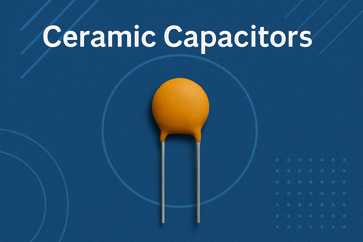
When an edge sensor or industrial actuator logs telemetry, runtime hours, or diagnostic counters directly to non-volatile memory, it exposes the device to premature hardware wear-out. An unmitigated write loop updating an internal state variable every few seconds can exhaust standard Electrically Erasable Programmable Read-Only Memory (EEPROM) silicon in weeks, resulting in bricked units or silently corrupted configuration parameters.Calculating real-world EEPROM operational lifespan requires modeling physical silicon wear against your firmware's write architecture, environmental operating profile, and hardware brownout defenses.Executive Overview: The First-Order Lifespan FormulaThe baseline lifespan of a single EEPROM memory cell is governed by the ratio of manufacturer-specified endurance to your system's cumulative annual write frequency:Lifespan (Years)=NratedWannual=NratedWday×365.25Where:Nrated is the manufacturer's qualified endurance limit per memory location (typically 105 to 106 write/erase cycles under nominal conditions).Wannual is the total number of physical erase/write cycles committed to that specific memory cell per calendar year.Wday is the average number of physical write events targeting the cell in a 24-hour window.Example calculation for a runtime counter written once per minute directly to a fixed address:Wday=60 writes/hr×24 hrs=1,440 writes/dayWannual=1,440×365.25=525,960 writes/yearAt a Nrated of $1{,}000{,}000$ cycles: Lifespan=1,000,000/525,960=1.90 YearsWhy the First-Order Formula Fails in Field DeploymentsRelying solely on this naive formula in commercial or industrial hardware risks field failures. The baseline calculation makes three flawed assumptions:It assumes byte writes only wear the target byte. On modern page-organized serial EEPROMs, writing a single byte cycles an entire internal physical page buffer (e.g., 32 or 64 bytes), multiplying wear on neighboring variables.It treats endurance and data retention as independent constants. Datasheet headlines advertising "$1{,}000{,}000$ write cycles" and "100-year data retention" are orthogonal boundary ratings. After $1{,}000{,}000$ cycles, data retention at elevated temperatures (85∘C to 125∘C) can degrade to single-digit months.It assumes static memory allocation. Without active wear leveling or conditional update suppression in firmware, cycle exhaustion concentrates on fixed pointer addresses and state counters.Engineering Decision Framework: Write Frequency vs. ArchitectureTo match system write patterns with the appropriate non-volatile memory architecture, use the following operational bounds:Update rate <1 event per hour: Standalone Serial EEPROM with software conditional updates (read-before-write pattern). No wear leveling required.Update rate 1 to 60 events per hour: Standalone Serial EEPROM with page-aligned circular buffer wear leveling and dual-bank ping-pong integrity protection.Update rate >1 event per minute up to continuous telemetry (>1 Hz): Transition hardware from EEPROM to Ferroelectric RAM (FRAM) or EERAM. Alternatively, cache state variables in volatile SRAM and flush to Flash/EEPROM only during controlled shutdown or brownout detection events.1. Silicon Wear Mechanics: Decoupling Write Endurance from Data RetentionEEPROM storage cells rely on a floating-gate or charge-trap transistor architecture. Programming and erasing require transporting electrons across an energy barrier formed by an ultra-thin silicon dioxide (SiO2) dielectric layer via Fowler-Nordheim (FN) quantum tunneling.Applying an internal programming potential (typically 12 V to 20 V, stepped up from the chip's 1.8 V–5.5 V supply rail via an on-chip charge pump) forces electrons through the dielectric barrier and onto the floating gate.Each tunnel cycle subjects the crystalline lattice of the SiO2 tunnel oxide to high electrical field stress (≈10 MV/cm). This stress generates atomic-scale defects:Interface trap generation: Dangling bonds form at the silicon-dielectric boundary.Oxide electron trapping: Electrons become permanently stuck inside the dielectric bulk, permanently shifting the cell's natural threshold voltage.Programming window collapse (ΔVt): The differential voltage between an erased state (logical 1) and a programmed state (logical 0) narrows over cumulative cycles until internal sense amplifiers can no longer distinguish between states.The Decoupling Myth: Endurance vs. Data RetentionNon-volatile qualification is governed by standards such as JEDEC JESD22-A117E (Electrically Erasable Programmable ROM Program / Erase Endurance and Data Retention Stress Test). A common architectural mistake is reading datasheet parameters as unlinked capabilities:Write Endurance: The cumulative count of erase/program transitions a cell can execute before dielectric wear-out or window collapse prevents reliable state programming.Data Retention: The span of time a written charge remains securely trapped on the floating gate without leaking back into the substrate when the chip is unpowered.When an EEPROM is brand new (uncycled), its tunnel oxide is free of trap pathways. JEDEC qualification shows uncycled cells can retain stored charge for 100 to 200 years at 25∘C.However, as a cell accumulates hundreds of thousands of write cycles, micro-structural defects form conductive leakage paths across the dielectric layer (stress-induced leakage current, or SILC). If an EEPROM is cycled to its maximum rated limit of 10^6 cycles[1] and then placed in an unpowered industrial cabinet at 85∘C, the retained charge will leak across these defect pathways. Real-world retention under those conditions can decline to under 5 years.Post-cycling data retention declines sharply at elevated temperatureNote on Read Cycling: Read operations use standard logic bias voltages without activating the high-voltage charge pump. Reading EEPROM addresses creates zero Fowler-Nordheim stress and zero dielectric wear. Read cycle endurance is functionally unlimited, though active reads draw standard dynamic bus operating current (ICC\_read).2. Architectural Granularity & Write Amplification: The Cost of Page BuffersHistorically, legacy parallel EEPROMs featured isolated select transistors per byte, allowing true random byte-level erasing and reprogramming without touching adjacent cells.To reduce silicon die size and lower pin counts, modern serial EEPROMs (e.g., standard I2C 24LCxx or SPI 25LCxx series) organize their memory arrays into physical pages. Common page boundaries are 16, 32, 64, or 128 bytes depending on density:Density / Part FamilyInterfaceTypical Physical Page SizeMaximum Self-Timed Write Time (tWC / tWR)24LC04 / 24LC08I2C16 Bytes5.0 ms24LC64 / 24AA64I2C32 Bytes5.0 ms24LC256 / 25LC256I2C / SPI64 Bytes5.0 ms24LC512 / 25LC512I2C / SPI128 Bytes5.0 msThe Write Amplification Factor (WAF)When firmware sends an I2C command to write a single byte to an address inside a page-buffered EEPROM, the device performs the following sequence internally:The address is decoded to identify the corresponding physical page.The entire physical page (e.g., 32 bytes) is loaded into an internal volatile SRAM page buffer.The addressed byte is modified within the buffer.The internal charge pump engages, triggering a self-timed erase/program cycle across the entire 32-byte physical array sector simultaneously.Updating a single 1-byte counter 100,000 times does not isolate wear to that single address. It subjects all adjacent bytes within that 32-byte physical page boundary to 100,000 full-voltage thermal/tunneling cycles.To quantify this wear, we define the Write Amplification Factor ($WAF$):WAF=Bytes physically cycled inside siliconBytes modified by firmwareFor unaligned or isolated parameter writes:WAF=SizepageSizepayload Weffective=Wraw×WAFIf a firmware engineer places a 4-byte system uptime variable and a 28-byte factory calibration table on the same 32-byte physical page of a Microchip 24LC64, each 4-byte update generates an effective write amplification factor:WAF=32 bytes4 bytes=8.0Updating the 4-byte counter 500,000 times subjects the factory calibration coefficients to 500,000 physical rewrite cycles, exhausting the entire page's endurance budget. Page-buffer wear amplification is one of the mechanisms documented in Microchip's Total Endurance modeling guide[6].A single-byte write cycles the entire physical page buffer3. Thermal Acceleration & The Fallacy of Flat Safety MarginsA frequent rule of thumb suggests applying an arbitrary "50% safety margin" to EEPROM cycle budgets. While well-intentioned, this heuristic lacks physical grounding in semiconductor reliability engineering. Mission-critical industrial and automotive systems budget endurance using the physics of dielectric breakdown, Arrhenius thermal models, and targeted parts-per-million (PPM) failure rates.Arrhenius Reaction Rate Modeling for Retention LossThermal charge dissipation from a degraded floating gate into oxide traps is governed by the Arrhenius equation:Acceleration Factor (AF)=tusetstress=exp[EakB(1Tuse−1Tstress)]Where:Ea is the apparent activation energy of the failure mode. For silicon dioxide dielectric defect wear-out and electron detrapping, Ea typically ranges between 0.6 eV (defect oxide conduction per ESA ECSS-Q-ST-30-11C) and 1.1 eV (thermal charge detrapping per JEDEC standards and Renesas qualification models).kB is Boltzmann's constant (8.617×10⁻⁵ eV/K).Tuse and Tstress are operating and qualification temperatures expressed in Kelvin (K=∘C+273.15).Worked example comparing charge retention at an operating junction temperature of 85∘C (358.15 K) against a baseline room qualification temperature of 25∘C (298.15 K) with Ea=0.8 eV:AF=exp[(0.8/(8.617×10−5))×((1/298.15)−(1/358.15))]AF=exp[9283.98×0.0005615]=exp[5.213]≈183.6In this system, thermal charge leakage accelerates by a factor of roughly 184x at 85∘C relative to room temperature. A cell retaining charge for 20 years at room temperature post-cycling may hold that charge for less than 40 days if cycled to its structural endurance limit and run continuously inside an unventilated 85∘C industrial control housing.The Dual Thermal TrapsReliability modeling must account for conditions at both temperature extremes:The High-Temperature Trap (>85∘C): Elevated lattice vibrations increase electron mobility through oxide traps, causing retention loss and premature window closure.The Low-Temperature Trap (<0∘C): Colder temperatures decrease electron thermal agitation, which increases the effective tunneling barrier height. Internal charge-pump circuits must generate higher peak programming potentials to move identical charge packets, increasing physical oxide lattice stress during write events.When specifying components for harsh environments, rely on qualification standards like AEC-Q100 Grade 1 (−40∘C to +125∘C) or Grade 2 (−40∘C to +105∘C), and request vendor-specific endurance-versus-retention qualification curves.Enterprise Explained – SSD Testing Endurance and Reliability4. Firmware Mitigation Architecture: Circular Buffering, Conditional Updates, and CoalescingFirmware structure directly dictates silicon lifespan. Three design patterns can reduce raw EEPROM write cycles by two to four orders of magnitude.Pattern 1: Conditional Update Suppression (update() vs. write())In microcontroller firmware, writing configuration variables on a fixed timer often commits identical data repeatedly. A conditional write routine executes a bus read first, performs a bitwise comparison in RAM, and initiates a physical write only if a bit mismatch is detected:#include <stdbool.h>#include <stdint.h>// Returns true if physical bus write was executed, false if suppressedbool eeprom_conditional_update(uint16_t mem_addr, const uint8_t *new_data, uint16_t len) { uint8_t current_val; bool write_needed = false; for (uint16_t i = 0; i < len; i++) { current_val = eeprom_hw_read_byte(mem_addr + i); if (current_val != new_data[i]) { write_needed = true; break; } } if (write_needed) { // Issue physical page or byte write cycle over I2C/SPI eeprom_hw_write_page(mem_addr, new_data, len); return true; } return false; // Suppressed: Saved one full internal physical write cycle}For quasi-static variables (such as network IP settings, calibration coefficients, or user presets), conditional updates eliminate $95\%$ to $99.9\%$ of raw write cycles.Pattern 2: Circular Buffer Wear LevelingFor dynamic variables that increment continuously (runtime hours, cycle counters, boot logs), writing to a static address will destroy that memory location. By allocating a contiguous pool of M slots aligned to physical page boundaries, wear is distributed evenly across the array.Lifespanleveled=Lifespansingle\_cell×M×ηoverheadWhere ηoverhead represents metadata utilization efficiency (typically 0.85 to 0.95 due to validation headers and CRC bytes).Instead of tracking the active slot using a dedicated "pointer address" (which would wear out on its own), use a monotonic sequence counter (Sseq) embedded in each record header to rebuild the state during initialization.typedef struct __attribute__((packed)) { uint32_t sequence_id; // Monotonically increasing counter uint32_t run_time_sec; // Payload data uint8_t payload[20]; // State metrics uint32_t crc32; // Integrity check over header + payload} eeprom_log_record_t; // Exactly 32 bytes (matches 24LC64 page size)#define BUFFER_SLOTS 32 // 32 slots * 32 bytes = 1024 bytes total allocation// Linear search on boot to locate the most recent valid recordint find_active_tail_slot(void) { uint32_t max_seq = 0; int tail_idx = -1; eeprom_log_record_t rec; for (int i = 0; i < BUFFER_SLOTS; i++) { eeprom_hw_read(i * sizeof(eeprom_log_record_t), (uint8_t*)&rec, sizeof(rec)); if (verify_crc32((uint8_t*)&rec, sizeof(rec) - 4) == rec.crc32) { if (rec.sequence_id >= max_seq) { max_seq = rec.sequence_id; tail_idx = i; } } } return tail_idx; // Returns current active head; next write goes to (tail_idx + 1) % BUFFER_SLOTS}Architectural Cost: Wear leveling trades silicon storage density for endurance. Allocating 32 slots extends write life by 32×, but divides available payload storage by 32.Pattern 3: RAM Shadow Caching & Shutdown CoalescingFor fast-changing parameters, maintain the authoritative state in volatile MCU SRAM. Commit the cache to EEPROM only when:A configuration transaction completes.A periodic background interval expires (e.g., once every 30 minutes).An early-warning Brown-Out Reset (BOR) interrupt signals an imminent DC rail drop.5. Hardware Protection: Power-Loss Integrity and the Programming WindowStandard serial EEPROMs are not instantaneous storage devices. When an I2C/SPI master issues a stop bit, the device starts an internal, self-timed programming window that typically takes 3.0 ms to 5.0 ms (datasheet maximum: up to 10.0 ms).If the VCC rail drops below the chip's minimum operational threshold (Vmin) during this window, the charge pump will collapse. This causes partial Fowler-Nordheim charge transfer, leaving floating gates in an intermediate, floating threshold state. The result is corrupted bits across the entire target page, not just the single byte being modified.Sizing the Brown-Out Hold-Up CapacitorTo guarantee write integrity through power loss, the power rail must sustain sufficient voltage until the worst-case programming cycle finishes:Chold≥Isystem×twrite\_maxVBOR−VminWhere:Isystem is the total active current drawn from the hold-up rail (including the EEPROM's active programming current Iwrite, MCU deep-sleep/BOR current, and quiescent leakage).twrite\_max is the manufacturer's maximum self-timed programming window (typically 5.0 ms for modern I2C EEPROMs like the Microchip 24LC64).VBOR is the trip point of the microcontroller's Brown-Out Reset circuit.Vmin is the minimum operational voltage rating of the EEPROM and MCU (e.g., 1.8 V or 2.5 V).Worked calculation:Total current during power-fail shutdown: Isystem=4.0 mA (EEPROM Iwrite=3.0 mA, MCU core =1.0 mA)Worst-case programming window: twrite\_max=5.0 msMCU BOR Trip Point: VBOR=2.7 VMinimum EEPROM rail voltage: Vmin=2.2 VDelta V=2.7 V−2.2 V=0.5 VChold≥(4.0 mA×5.0 ms)/0.5 VChold≥(0.004 A×0.005 s)/0.5 V=0.000040 Farads=40.0 μFSelection: Place a standard 47 μF or 100 μF low-ESR ceramic capacitor on the isolated local memory rail.Firmware Defense: Dual-Bank "Ping-Pong" CommitHardware capacitance should be paired with a dual-bank ping-pong architecture in firmware. Storage is divided into Bank A and Bank B. The MCU never overwrites the active configuration in place.Write new data, an incremented sequence ID, and a fresh CRC-32 checksum to the inactive bank.Verify the write completes.If power fails mid-cycle, the newly written bank fails its CRC check on restart, and the system falls back to the previous intact bank.Dual-bank ping-pong commit protects configuration through power loss6. Memory Migration Boundaries: Quantitative Selection MatrixWhen write logging exceeds standard EEPROM cycle life, or when 5 ms write latencies compromise real-time control loops, updating the hardware architecture is more reliable than writing complex firmware workarounds.Technology Comparison MatrixTechnical ParameterStandalone Serial EEPROMInternal MCU Flash EmulationFerroelectric RAM (FRAM)EERAM / nvSRAMTypical Write Endurance105 to 106 cycles104 to 105 sector erases1013 to 1014 cycles106 store events (unlimited SRAM writes)Write Latency3.0 to 10.0 ms (self-timed)2.0 to 40.0 ms (sector erase delay)Sub-150 ns (bus speed, zero delay)Sub-50 ns (direct SRAM write access)Write GranularityByte alterable / Page buffer (16–64B)Sector / Block erase (512B–4KB)True Random Byte / WordTrue Random Byte / WordEnergy Consumption per WriteModerate (≈3,900 μJ for 64 Kb)High (high-voltage bulk sector erase)Ultra-low (≈17 μJ for 64 Kb)Low (standard SRAM bus level)Power-Loss VulnerabilityHigh during 5 ms programmingHigh during block erase/re-writeLow (ferroelectric state latch)Zero (auto-store capacitor drives transfer)Driver ComplexityLow (standard I2C/SPI commands)High (requires wear-leveling driver)Low (drop-in I2C/SPI SRAM style)Low to Medium (requires store trigger setup)Relative Unit BOM CostLow baselineLowest ($0 incremental BOM)HighMedium-HighWrite energy comparison note: Qualification data from Infineon Technologies reveals that writing a 64 Kb block to standard serial EEPROM consumes roughly 3,900 μJ due to internal charge-pump duration. An equivalent EXCELON F-RAM device completes the operation in bus time using roughly 17 μJ—a 229x reduction in write energy[4] that can significantly extend battery runtime in low-power edge designs.Concrete Migration Decision TreesYES — Is continuous telemetry logging required (update interval < 1.0 second)? Switch to FRAM or EERAM. Endurance of 1014 cycles allows continuous high-speed writes without wear.NO — Continue evaluating below.YES — Is parameter storage footprint > 64 Kilobytes with large batch updates? Switch to External NOR Flash running a wear-leveling filesystem (e.g., LittleFS).NO — Continue evaluating below.YES — Are total lifetime updates < 50,000 events, with zero additional BOM cost tolerance? Use Internal MCU Flash Emulation with dual-sector rotation (e.g., ST AN3969[3]).NO — Use Standalone Serial EEPROM (e.g., Microchip 24LCxx / ST M24xx).7. Step-by-Step EEPROM Write Budget Worksheet & Industrial Case StudyTo build an endurance budget, audit every application data structure by its payload size, update rate, physical page alignment, and wear-leveling multiplier.Worked Example: Industrial Smart ActuatorTarget System Lifetime: 10 years continuous 24/7 industrial operation (87,660 hours).Memory Device Selected: Microchip 24LC64 (64 Kbit / 8 KB I2C EEPROM, 32-byte physical page size, $Sources and references used for this guideAN1019: EEPROM Endurance TutorialSource type: official company documentationUsed for: Physical endurance mechanisms, write cycle definitions, cell degradation, and application write pattern analysis.Caution: Vendor technical application note; focuses primarily on Microchip silicon architectures and qualification test standards.AN5866: Guidelines for cycling endurance and data retention of page EEPROMsSource type: official company documentationUsed for: Page-based endurance budgeting, mathematical wear modeling, write amplification factor across page boundaries, and retention decay curves.Caution: Vendor documentation; specific page boundaries and buffer architectures must be verified against individual part datasheets.AN3969: EEPROM emulation in STM32F40x/STM32F41x microcontrollersSource type: official company documentationUsed for: MCU internal Flash EEPROM emulation mechanics, sector swapping, erase cycle wear modeling, and comparison with dedicated EEPROM.Caution: Vendor implementation guide; reflects internal NOR Flash endurance characteristics (10k-100k cycles) rather than standalone EEPROM.FRAM or Flash: How to Select the Right MCU for Your Application (sszta32)Source type: official company documentationUsed for: Comparative trade-offs between Ferroelectric RAM (FRAM), Flash, and EEPROM regarding endurance (10^14 cycles), write latency, and energy per write.Caution: Vendor whitepaper authored by Texas Instruments; naturally highlights FRAM technology strengths.AN1095: Emulating Data EEPROM for PIC18 and PIC24 MicrocontrollersSource type: official company documentationUsed for: Virtual EEPROM wear leveling, Flash memory row/sector allocation, and write-cycle consumption analysis.Caution: Focuses on PIC MCU Flash architectures; design patterns apply conceptually but specific register structures vary.Total Endurance v5.00 Quick Start Guide (51342B)Source type: official company documentationUsed for: Page-mode write cycle penalties, byte-in-page write amplification, and endurance modeling software mechanics.Caution: Refers to legacy simulation tools, but the underlying page-write wear physics and mathematical relationships remain fully valid.AN6604: Using the Microchip Endurance Predictive SoftwareSource type: official company documentationUsed for: Predictive modeling of write patterns, cumulative probability of failure, and statistical cell endurance distributions.Caution: Vendor proprietary software application note; useful for reliability theory and statistical distribution models.AN798: EEPROM Emulation with Wear-Leveling for 8-Bit MicrocontrollersSource type: official company documentationUsed for: Firmware circular buffer architectures, dynamic sequence numbering, virtual-to-physical mapping, and avoiding static pointer burnout.Caution: Tailored for resource-constrained 8-bit devices; algorithms must be adapted for 32-bit platforms and high-concurrency RTOS tasks.
On 2026-09-30