The Kynix Components - Discrete Semiconductor Products
Stay Ahead with Expert Electronics Insights,
Industry Trends, and Innovative Tips
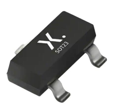
CatalogProduct OverviewFDV301N Related Video IntroductionFDV301N CAD ModelsFDV301N Pin configurationFDV301N Marking DiagramFDV301N Package DimensionsFDV301N FeaturesFDV301N Inverter ApplicationFDV301N DatasheetFDV301N SpecificationsFDV301N ManufacturerUsing WarningFDV301N FAQ Product OverviewThis N−Channel logic level enhancement mode field effect transistor is produced using onsemi’s proprietary, high cell density, DMOS technology. This very high density process is especially tailored to minimize on−state resistance. This device has been designed especially for low voltage applications as a replacement for digital transistors. Since bias resistors are not required, this one N−channel FET can replace several different digital transistors, with different bias resistor values. FDV301N Related Video IntroductionFDV301N Video Description: Step by step Testing Tutorial N-Channel P-Channel Mosfet using Digital Multimeter. FDV301N CAD ModelsFigure: FDV301N PCB Symbol Figure: FDV301N Footprint Figure: FDV301N 3D Models FDV301N Pin configurationFigure: FDV301N PinoutFDV301N is a three pin device as shown in figure and the function of each of those pins is stated below. PinNameFunction1DrainCurrent comes in to the device from this pin.2GateMOSFET gets turned ON and OFF depending on voltage applied at this pin.3SourceCurrent which comes in to the device goes out through this pin. This pin is usually connected to ground. FDV301N Marking DiagramFigure: FDV301N Marking Diagram &E = Designates Space&Y = Binary Calendar YearCoding Scheme301 = Specific Device Code&G = Date Code FDV301N Package DimensionsFigure: FDV301N Package Dimensions FDV301N Features25 V, 0.22 A Continuous, 0.5 A Peak♦ RDS(on) = 5 @ VGS = 2.7 V♦ RDS(on) = 4 @ VGS = 4.5 VVery Low Level Gate Drive Requirements Allowing Direct Operation in 3 V Circuits. VGS(th) < 1.06 VGate−Source Zener for ESD Ruggedness. > 6 kV Human BodyModelReplace Multiple NPN Digital Transistors with One DMOS FETThis Device is Pb−Free and Halide Free FDV301N Inverter ApplicationFigure: FDV301N Inverter Application FDV301N DatasheetYou can download the datasheet from the link given below:FDV301N Datasheet FDV301N SpecificationsProduct AttributeAttribute ValueManufacturer:onsemiProduct Category:MOSFETTechnology:SiMounting Style:SMD/SMTPackage / Case:SOT-23-3Transistor Polarity:N-ChannelNumber of Channels:1 ChannelVds - Drain-Source Breakdown Voltage:25 VId - Continuous Drain Current:220 mARds On - Drain-Source Resistance:5 OhmsVgs - Gate-Source Voltage:- 8 V, + 8 VVgs th - Gate-Source Threshold Voltage:700 mVQg - Gate Charge:700 pCOperating Temperature:-55°C ~ 150°C (TJ)Pd - Power Dissipation:350 mWChannel Mode:EnhancementBrand:onsemi / FairchildConfiguration:SingleFall Time:6 nsForward Transconductance - Min:0.2 SHeight:1.2 mmLength:2.9 mmProduct:MOSFET Small SignalProduct Type:MOSFETRise Time:6 nsSeries:FDV301NSubcategory:MOSFETsTransistor Type:1 N-ChannelType:FETTypical Turn-Off Delay Time:3.5 nsTypical Turn-On Delay Time:3.2 nsWidth:1.3 mmPart # Aliases:FDV301N_NLUnit Weight:0.000282 oz FDV301N ManufacturerOnsemi is driving energy efficient innovations, empowering customers to reduce global energy use. The company offers a comprehensive portfolio of energy efficient power and signal management, logic, discrete and custom solutions to help design engineers solve their unique design challenges in automotive, communications, computing, consumer, industrial, LED lighting, medical, military/aerospace and power supply applications. onsemi operates a responsive, reliable, world-class supply chain and quality program, and a network of manufacturing facilities, sales offices and design centers in key markets throughout North America, Europe, and the Asia Pacific regions. Using WarningNote: Please check their parameters and pin configuration before replacing them in your circuit. FDV301N FAQWhat is FDV301N?FDV301N is semiconductor device called MOSFET (Metal Oxide Semiconductor Field Effect Transistor) and is used as a high speed switching device in applications. The device is an N-Channel enhancement mode Field Effect Transistor that is produced using ON Semiconductor's proprietary, high cell density, DMOS technology. What does N channel mean?Channel MOSFET is a type of metal oxidesemiconductor field-effect transistorthat is categorized under the field-effect transistors (FET). This type of transistor is also known as an insulated-gate field-effect transistor (IGFET). Sometimes it is also known as a metal-insulator field-effect transistor (MIFET). What is N and P channel?N channel MOSFETs are fast switching devices. The N channel MOSFETs are TTL compatible. As the applied gate voltage and drain supply are positive for an n-channel enhancement MOSFET. The drain resistance of P channel MOSFET is 3 times higher than that for an identical N-channel MOSFET.
Kynix On 2021-12-03
Product OverviewThe IRF740 is an N-Channel Power MOSFET which can switch loads upto 400V. The Mosfet could switch loads that consume upto 10A, it can turned on by provide a gate threshold voltage of 10V across the Gate and Source pin. Since the mosfet is for switching high current high voltage loads it has a relatively high gate voltage, hence cannot be used directly with a I/O pin of a CPU. This blog will introduce IRF740systematically from its features, pinout to its specifications, applications, also including IRF740 datasheet and so much more. CatalogProduct OverviewRelated Video IntroductionIRF740 FeaturesIRF740 PinoutPin ConfigurationIRF740 ApplicationsIRF740 EquivalentsIRF740 Circuit DiagramIRF740 PackageIRF740 SpecificationIRF740 ManufacturerIRF740 DatasheetUsing WarningsIRF740 FAQ Related Video Introduction Video: MOSFET IRF740 (getting to know it) IRF740 Video Description: My first look at a MOSFET, so just a basic circuit to test it out as a switch for a motor. IRF740 FeaturesDynamic dV/dt ratingRepetitive avalanche ratedFast switchingEase of parallelingSimple drive requirements IRF740 PinoutThe following figure is the diagram of IRF740 pinout. IRF740 Pinout Pin ConfigurationPin NumberPin NameDescription1SourceCurrent flows out through Source (maximum 10A)2GateControls the biasing of the MOSFET (Threshold voltage 10V)3DrainCurrent flows in through Drain IRF740 ApplicationsSwitching high power devicesInverter CircuitsDC-DC ConvertersControl speed of motorsLED dimmers or flashersHigh Speed switching applications IRF740 EquivalentsIRFB13N50A, UF450A, SSF13N15 IRF740 Circuit DiagramThe following is the circuit diagram of IRF740. Switching Time Test Circuit 13b - Gate Charge Test Circuit IRF740 PackageThe following diagram shows the IRF740package. IRF740 Package IRF740 SpecificationProduct AttributeAttribute ValueManufacturer:STMicroelectronicsProduct Category:MOSFETTechnology:SiMounting Style:Through HolePackage / Case:TO-220-3Transistor Polarity:N-ChannelNumber of Channels:1 ChannelVds - Drain-Source Breakdown Voltage:400 VId - Continuous Drain Current:10 ARds On - Drain-Source Resistance:550 mOhmsVgs - Gate-Source Voltage:- 20 V, + 20 VMinimum Operating Temperature:- 65 CMaximum Operating Temperature:+ 150 CPd - Power Dissipation:125 WChannel Mode:EnhancementPackaging:TubeConfiguration:SingleForward Transconductance - Min:4 SHeight:9.15 mmLength:10.4 mmRise Time:10 ns IRF740 ManufacturerSTMicroelectronics is a global independent semiconductor company and a leader in developing and delivering semiconductor solutions across the spectrum of microelectronics applications. An unrivaled combination of silicon and system expertise, manufacturing strength, Intellectual Property (IP) portfolio, and strategic partners positions, STMicroelectronics is at the forefront of System-on-Chip (SoC) technology and its products play a key role in enabling today's convergence trends. IRF740 DatasheetYou can download IRF740 datasheet from the link given below:IRF740 Datasheet Using WarningsNote: Please check their parameters and pin configuration before replacing them in your circuit. IRF740 FAQWhat is IRF740?The IRF740 is an N-Channel Power MOSFET which can switch loads upto 400V. The Mosfet could switch loads that consume upto 10A, it can turned on by provide a gate threshold voltage of 10V across the Gate and Source pin. Hence this mosfet cannot be used in applications where high switching efficiency is required. What are MOSFET transistors used for?The purpose of a MOSFET transistor is essentially to control voltage/current flow between the source and the drain. What is N-channel Mosfet?A N-Channel MOSFET is a type of MOSFET in which the channel of the MOSFET is composed of a majority of electrons as current carriers. When the MOSFET is activated and is on, the majority of the current flowing are electrons moving through the channel. What are power MOSFETs used for?Power MOSFETs are widely used in transportation technology, which include a wide range of vehicles. In the automotive industry, power MOSFETs are widely used in automotive electronics. Power MOSFETs (including DMOS, LDMOS and VMOS) are commonly used for a wide range of other applications. How does N-channel MOSFET transistor work?The working of the n-channel MOSFET is based on the majority of the carriers that are electrons. These electrons move in the channel is responsible for the flow of current in the transistor. The p-substrate material is required in the formation of the gate terminals.
Kynix On 2021-12-02
CatalogProduct OverviewBSS123 Related Video IntroductionBSS123 CAD ModelsBSS123 Marking DiagramBSS123 Package DimensionsBSS123 FeaturesBSS123 ApplicationsBSS123 DatasheetBSS123 SpecificationsBSS123 ManufacturerUsing WarningBSS123 FAQ Product OverviewThese N−Channel enhancement mode field effect transistors are produced using onsemi’s proprietary, high cell density, DMOS technology. These products have been designed to minimize on−state resistance while provide rugged, reliable, and fast switching performance. These products are particularly suited for low voltage, low current applications such as small servo motor control, power MOSFET gate drivers, and other switching applications. BSS123 Related Video IntroductionBSS123 Video Description: Today I am going to explain you about N-Channel logic level enhancement mode power field effect transistor. we learn why used in laptop this smd component. BSS123 CAD ModelsFigure: BSS123 PCB Symbol Figure: BSS123 Footprint Figure: BSS123 3D Models BSS123 Marking DiagramFigure: BSS123 Marking DiagramSA = Specific Device CodeM = Date Code*(Note: Microdot may be in either location)*Date Code orientation and/or position may vary depending upon manufacturing location. BSS123 Package DimensionsFigure: BSS123 Package Dimensions BSS123 Features0.17 A, 100 V♦ RDS(on) = 6 @ VGS = 10 V♦ RDS(on) = 10 @ VGS = 4.5 VHigh Density Cell Design for Extremely Low RDS(on)Rugged and ReliableCompact Industry Standard SOT−23 Surface Mount PackageThis Device is Pb−Free and Halogen Free BSS123 DatasheetYou can download the datasheet from the link given below:BSS123 Datasheet BSS123 SpecificationsProduct AttributeAttribute ValueManufacturer:onsemiProduct Category:MOSFETTechnology:SiMounting Style:SMD/SMTPackage / Case:SOT-23-3Transistor Polarity:N-ChannelNumber of Channels:1 ChannelVds - Drain-Source Breakdown Voltage:100 VId - Continuous Drain Current:170 mARds On - Drain-Source Resistance:6 OhmsVgs - Gate-Source Voltage:- 20 V, + 20 VVgs th - Gate-Source Threshold Voltage:800 mVQg - Gate Charge:2.5 nCOperating Temperature:-55°C ~ 150°C (TJ)Pd - Power Dissipation:300 mWChannel Mode:EnhancementBrand:onsemi / FairchildConfiguration:SingleFall Time:9 nsForward Transconductance - Min:0.8 SHeight:1.2 mmLength:2.9 mmProduct:MOSFET Small SignalProduct Type:MOSFETRise Time:9 nsSeries:BSS123Subcategory:MOSFETsTransistor Type:1 N-ChannelType:FETTypical Turn-Off Delay Time:17 nsTypical Turn-On Delay Time:1.7 nsWidth:1.3 mmPart # Aliases:BSS123_NLUnit Weight:0.000282 oz BSS123 ManufacturerOnsemi is driving energy efficient innovations, empowering customers to reduce global energy use. The company offers a comprehensive portfolio of energy efficient power and signal management, logic, discrete and custom solutions to help design engineers solve their unique design challenges in automotive, communications, computing, consumer, industrial, LED lighting, medical, military/aerospace and power supply applications. onsemi operates a responsive, reliable, world-class supply chain and quality program, and a network of manufacturing facilities, sales offices and design centers in key markets throughout North America, Europe, and the Asia Pacific regions. Using WarningNote: Please check their parameters and pin configuration before replacing them in your circuit. BSS123 FAQWhat is BSS123?The BSS123 is an N-Channel Logic Level Enhancement Mode Field Effect Transistor that comes in surface mount package SOT-23. It is a rugged and reliable device that comes with a drain-source voltage of around 100V while the gate-source voltage is -+20V. What is an N-channel enhancement mode MOSFET?In n-channel enhancement mode, no current flows through the transistor until the voltage at the gate and terminal source exceed the minimum voltage cut in value. If the voltage at the drain and the terminal source is applied then even there is no evident flow of the current. What are the two main types of field effect transistors?There are two types of field-effect transistors, the Junction Field-Effect Transistor (JFET) and the “Metal-Oxide Semiconductor” Field-Effect Transistor (MOSFET), or Insulated-Gate Field-Effect Transistor (IGFET).
Kynix On 2021-12-02
CatalogProduct OverviewBD139 Related Video IntroductionBD139 CAD ModelsBD139 Internal Schematic DiagramBD139 Packaging DimensionsBD139 FeaturesBD139 ApplicationsBD139 DatasheetBD139 SpecificationsBD139 ManufacturerUsing WarningBD139 FAQ Product OverviewThese epitaxial planar transistors are mounted in the SOT-32 plastic package. They are designed for audio amplifiers and drivers utilizing complementary or quasi-complementary circuits. The NPN types are the BD135 and BD139, and the complementary PNP types are the BD136 and BD140. BD139 Related Video IntroductionBD139 Video Description: How to make Auto ON OFF Led light use NPN BD139, diy dark sensorToday i will show you how to make automatic on and off led light using npn transistor bd139 and LDR sensor, diy dark sensor simple and easy electronics projects make at home.auto on off led light electronics project.I hopeful this video will be helpful for you and your friends please like,share and subscribe for more videos. BD139 CAD ModelsFigure: BD139 PCB Symbol Figure: BD139 Footprint Figure: BD139 3D Models BD139 Internal Schematic DiagramFigure: BD139 Internal Schematic Diagram BD139 Packaging DimensionsFigure: BD139 Packaging Dimensions BD139 Features■ Products are pre-selected in DC current gain BD139 Applications■ General purpose BD139 DatasheetYou can download the datasheet from the link given below:BD139 Datasheet BD139 SpecificationsProduct AttributeAttribute ValueManufacturer:STMicroelectronicsProduct Category:Bipolar Transistors - BJTMounting Style:Through HolePackage / Case:SOT-32-3Transistor Polarity:NPNConfiguration:SingleCollector- Emitter Voltage VCEO Max:80 VCollector- Base Voltage VCBO:80 VEmitter- Base Voltage VEBO:5 VCollector-Emitter Saturation Voltage:0.5 VMaximum DC Collector Current:1.5 APd - Power Dissipation:12.5 WMinimum Operating Temperature:- 65°CMaximum Operating Temperature:+ 150°CSeries:BD139Packaging:TubeBrand:STMicroelectronicsContinuous Collector Current:1.5 ADC Collector/Base Gain hfe Min:40DC Current Gain hFE Max:250Height:10.8 mmLength:7.8 mmProduct Type:BJTs - Bipolar TransistorsSubcategory:TransistorsTechnology:SiWidth:2.7 mmUnit Weight:0.002116 oz BD139 ManufacturerSTMicroelectronics is a French-Italian multinational electronics and semiconductors manufacturer headquartered in Plan-les-Ouates near Geneva, Switzerland. The company resulted from the merger of two government-owned semiconductor companies in 1987: "Thomson Semiconducteurs" of France and "SGS Microelettronica" of Italy. It is commonly called "ST", and it is Europe's largest semiconductor chip maker based on revenue. While STMicroelectronics corporate headquarters and the headquarters for EMEA region are based in the Canton of Geneva, the holding company, STMicroelectronics N.V. is incorporated in the Netherlands. Using WarningNote: Please check their parameters and pin configuration before replacing them in your circuit. BD139 FAQWhat is BD139?BD139 is a Bipolar NPN transistor, it is mounted in the SOT-32 plastic package. It is designed for audio amplifier and driver utilizing complementary circuits. BD139 has a gain value of 40 to 160, which determine the amplification capacity of a transistor. What is BD139 used for?A Bipolar NPN transistor like BD139 is available in the SOT-32 plastic package. This kind of transistor is used in different electronic circuits because of less cost and high collector current. This transistor can drive upto 1.5A loads like motors, high power LEDs, relays, etc. How does BD139 work?BD139 is a Bipolar NPN transistor, it is mounted in the SOT-32 plastic package. BD139 has a gain value of 40 to 160, which determine the amplification capacity of a transistor. It has three main pinouts which are a collector, base and emitter. It is used to control (On/Off) bigger loads that consume less than 1.5A.
Kynix On 2021-12-01
CatalogProduct OverviewULN2803A Related Video IntroductionULN2803A CAD ModelsULN2803A Schematic DiagramULN2803A Pin ConfigurationULN2803A Test circuitsULN2803A FeaturesULN2803A Package DimensionsULN2803A DatasheetULN2803A SpecificationsULN2803A ManufacturerUsing WarningULN2803A FAQ Product OverviewThe ULN2801A, ULN2802A, ULN2803A and ULN2804A each contain eight Darlington transistors with common emitters and integral suppression diodes for inductive loads. Each Darlington features a peak load current rating of 600 mA (500 mA continuous) and can withstand at least 50 V in the OFF state. Outputs may be paralleled for higher current capability. Four versions are available to simplify interfacing to standard logic families: the ULN2801A is designed for general purpose applications with a current limit resistor; the ULN2802A has a 10.5k input resistor and Zener for 14-25 V PMOS; the ULN2803A has a 2.7 kW input resistor for 5 V TTL and CMOS; the ULN2804A has a 10.5 k input resistor for 6-15 V CMOS. All types are supplied in an 18-lead plastic DIP with a copper lead form and feature the convenient input-opposite-output pinout to simplify board layout. ULN2803A Related Video IntroductionULN2803A Video Description: Give the output logic of your microcontroller projects more current and voltage to drive larger loads with this simple to use chip. ULN2803A CAD ModelsFigure: ULN2803A PCB Symbol Figure: ULN2803A Footprint Figure: ULN2803A 3D Models ULN2803A Schematic DiagramFigure: ULN2803A Schematic Diagram ULN2803A Pin ConfigurationFigure: ULN2803A Pin Configuration ULN2803A Test circuitsFigure: ULN2803A Output leakage current Figure: ULN2803A Collector-emitter saturation voltage Figure: ULN2803A Input current (ON) Figure: ULN2803A Input current (OFF) Figure: ULN2803A Input voltage ULN2803A FeaturesEight Darlington transistors with commonemittersOutput current to 500 mAOutput voltage to 50 VIntegral suppression diodesVersions for all popular logic familiesOutput can be paralleledInputs pinned opposite outputs to simplifyboard layout ULN2803A Package DimensionsFigure: ULN2803A Package Dimensions ULN2803A DatasheetYou can download the datasheet from the link given below:ULN2803A Datasheet ULN2803A SpecificationsProduct AttributeAttribute ValueManufacturer:STMicroelectronicsProduct Category:Darlington TransistorsConfiguration:OctalTransistor Polarity:NPNCollector- Emitter Voltage VCEO Max:50 VMaximum DC Collector Current:0.5 AMounting Style:Through HolePackage / Case:PDIP-18Operating Temperature:-20°C ~ 150°C (TJ)Series:ULN2803APackaging:TubeBrand:STMicroelectronicsContinuous Collector Current:500 mAHeight:3.68 mmLength:23.24 mmProduct Type:Darlington TransistorsSubcategory:TransistorsWidth:7.1 mmUnit Weight:0.045856 oz ULN2803A ManufacturerSTMicroelectronics is a French-Italian multinational electronics and semiconductors manufacturer headquartered in Plan-les-Ouates near Geneva, Switzerland. The company resulted from the merger of two government-owned semiconductor companies in 1987: "Thomson Semiconducteurs" of France and "SGS Microelettronica" of Italy. It is commonly called "ST", and it is Europe's largest semiconductor chip maker based on revenue. While STMicroelectronics corporate headquarters and the headquarters for EMEA region are based in the Canton of Geneva, the holding company, STMicroelectronics N.V. is incorporated in the Netherlands. Using WarningNote: Please check their parameters and pin configuration before replacing them in your circuit. ULN2803A FAQWhat is ULN2803A?The ULN2803A device is a 50 V, 500 mA Darlington transistor array. The device consists of eight NPN Darlington pairs that feature high-voltage outputs with common-cathode clamp diodes for switching inductive loads. The Darlington pairs may be connected in parallel for higher current capability. How does a ULN2803A work?The ULN2803 IC consists of eight NPN Darlington pair which provides the proper current amplification required by the loads. In this pair the current amplified by the first transistor is further amplified by the next transistor providing high current to the output terminal. What is the difference between ULN2803 and ULN2003?The biggest difference is the additional channel and the diode to protect from a spike. The data sheets do point out exactly what the difference is, but they are essentially both Darlington arrays ganged together in a Dip chip. What is use of ULN2803 in relay interfacing?Applications include a stepper motor, relay drivers, hammer drivers, lamp drivers, display drivers (LED and gas discharge), line drivers, and logic buffers. The ULN2803 has a 2.7-k series base resistor for each Darlington pair for operation directly with TTL or 5-V CMOS devices. What is a Darlington array?Darlington devices are high-voltage, high-current switch arrays containing multiple open-collector Darlington pairs or multiple Darlington transistors with common emitters, and integral suppression diodes for inductive loads.
Kynix On 2021-11-30
CatalogProduct OverviewPN2222A Related Video IntroductionPN2222A CAD ModelsPN2222A Packaging DimensionsPN2222A FeaturesPN2222A Mechanical DataPN2222A Maximum Ratings and Electrical CharacteristicsPN2222A ApplicationsPN2222A Special ConsiderationsPN2222A DatasheetPN2222A SpecificationsPN2222A ManufacturerUsing WarningPN2222A FAQ Product OverviewLike most transistors, the PN2222A can function as a transistor, switch, or amplifier. It is an NPN type transistor with an operating temperature range of -55 to 150 degrees Celsius. The component can dissipate 625 mW of power, giving it good thermal control for not being a MOSFET, which is designed for thermal dissipation. It has an extremely low switching delay time of 10 nanoseconds, potentially as low as 5 nanoseconds, which has likely contributed to its continued popularity. The PN2222A is commonly called a small signal transistor due to its low energy applications. Its PNP complementary type, which can function similarly, is PN2907A. Taking into account NPN variations, PNP complementary types, and transistors that function similarly, this overview can be applied to more than a dozen transistors. The PN2222A can be structured differently from the traditional transistor “jellyfish” shape, where three prongs extend downward from a solid base. Alternative structures have dramatically shorter prongs than normal transistors. One structure can place the base and emitter prongs on one side of a large rectangular base with the collector prong on the other. Another structure places the base, collector, and emitter prongs all on one side of the large rectangular base with a fourth, larger collector prong on the opposing side. These structures are more compact than a usual transistor and can save space in electronics projects. PN2222A Related Video IntroductionPN2222A Video Description: Video shows you how to hook up the BJT to a circuit and demo how it works. This is part of my LED cube 8x8x8 project I'm working on. PN2222A CAD ModelsFigure: PN2222A PCB Symbol Figure: PN2222A Footprint Figure: PN2222A 3D ModelsPN2222A Packaging DimensionsFigure: PN2222A Packaging Dimensions PN2222A FeaturesPower dissipation PCM: 625mW(Tamb=25℃)Collector current ICM: 0.6 ACollector-base voltage V(BR)CBO: 75 VOperating and storage junction temperature range TJ,Tstg: -55℃ to+150℃ PN2222A Mechanical Data * Case: Molded plastic* Epoxy: UL 94V-O rate flame retardant* Lead: MIL-STD-202E method 208C guaranteed* Mounting position: Any* Weight: 0.008 gram PN2222A Maximum Ratings and Electrical Characteristics Ratings at 25℃ ambient temperature unless otherwise specified.Single phase, half wave, 60 Hz, resistive or inductive load. For capacitive load, derate current by 20%. PN2222A ApplicationsThe PN2222A is suitable for televisions, consumer electronics, home appliances, and robotics. It has been commonly used in Arduino projects for more than a decade and can be paired with more robust transistors like MOSFETs. Complex projects for the Internet of Things (IoT) can also make use of the PN2222A. This last use is of particular interest, since it allows amateur electronics engineers to conceptualize IoT projects and democratize electronics development. PN2222A Special ConsiderationsThe PN2222A is not suited for applications that require extremely high operating temperatures or voltages, although it can handle high current loads. It is also important that designers not stress the PN2222A to its maximum ratings for an extended period of time. The PN2222A can switch between high current loads up to 800 mA, which distinguishes it from similar transistors. Different datasheets say that this current load could be significantly smaller, but compared to other transistors, the PN2222A always handles high current loads. The BC547 is similar to the PN2222A, but cannot handle the same high current loads. When choosing between the PN2222A and similar transistors, designers should be careful to choose one that can handle the current load their project requires. This is especially important when combining the PN2222A with another transistor to create a Darlington pair, which amplifies current through one transistor, then another, creating potentially greater current levels than one transistor could handle alone. Many different companies have created variants of the PN2222A, resulting in many datasheets detailing components with slightly different properties. Designers should make sure, when referencing a datasheet, to use the most recently available sheet that corresponds to the company that made their specific PN2222A. Current tolerances can vary significantly between companies, even though the component itself is specialized for higher current loads. PN2222A DatasheetYou can download the datasheet from the link given below:PN2222A Datasheet PN2222A SpecificationsProduct AttributeAttribute ValueManufacturer:RectronProduct Category:Bipolar Transistors - BJTMounting Style:Through HolePackage / Case:TO-92-3Transistor Polarity:NPNConfiguration:SingleCollector- Emitter Voltage VCEO Max:40 VCollector- Base Voltage VCBO:75 VEmitter- Base Voltage VEBO:6 VCollector-Emitter Saturation Voltage:1 VPd - Power Dissipation:625 mWGain Bandwidth Product fT:300 MHzMinimum Operating Temperature:- 55℃Maximum Operating Temperature:+ 150℃Packaging:ReelBrand:RectronDC Collector/Base Gain hfe Min:75DC Current Gain hFE Max:375Product Type:BJTs - Bipolar TransistorsSubcategory:TransistorsTechnology:Si PN2222A ManufacturerRECTRON is a leading manufacturer of power semiconductors, offering a comprehensive range of rectifiers including bridge rectifiers, switching diodes, zener diodes, signal transistors and transient voltage suppressors. Product technologies include schottky barrier, ultra fast, super fast, epitaxial, high efficiency, fast recovery, and standard recovery, which is available in a proprietary glass passivated junction construction that significantly increases long term and environmental reliability. All product technologies are produced in a variety of topologies and include axial lead ,SIP, DIP, CASE, surface mount, SOD, SMA, SMB, SMC, DIP, chip & die custom packages. Using WarningNote: Please check their parameters and pin configuration before replacing them in your circuit. PN2222A FAQWhat is PN2222A?The PN2222A, also known as the PN2222, is a general-purpose transistor best suited to applications that don't require high stress on the component. Depending on the datasheet, it is characterized as a transistor or an amplifier, but it can perform both of those functions. What is a transistor symbol?The Transistor is a semiconductor device provided with three terminals called base, emitter and collector. It is used to work in electronic circuits as a rectifier, amplifier and switch. These symbols can be represented inside a circle. What is a bipolar transistor?Bipolar transistors are a type of transistor composed of pn junctions, which are also called bipolar junction transistors (BJTs). Whereas a field-effect transistor is a unipolar device, a bipolar transistor is so named because its operation involves two kinds of charge carriers, holes and electrons. How does a bipolar transistor work?Bipolar transistors are current-controlled and operated devices, meaning that a much smaller base current causes a larger current to flow from emitter to collector. Whereas transformers can amplify either current or voltage, transistors can amplify both. What's the purpose of bipolar transistors?Bipolar transistors are still used for amplification of signals, switching, and in digital circuits. Specialized types are used for high voltage switches, for radio-frequency amplifiers, or for switching heavy currents.
Kynix On 2021-11-29
Join our mailing list!
Be the first to know about new products, special offers, and more.
Feature Posts
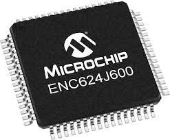
ENC624J600-I/PT microcontroller: Datasheet, Features, Application[FAQ]2023-03-07
ATMEGA1280-16AU microcontroller: Datasheet, Features, Application[FAQ]2023-03-07
STM8S207CBT6 Microcontroller: Datasheet, Features, Application[FAQ]2023-03-06
2N7002P Mosfet: Datasheet, Pinout, Features [FAQ]2021-10-21
L298N Motor Driver: Datasheet, Arduino, Circuit [Video&FAQ]2021-10-21