info@kynix.com
 00852-6915 1330


 0
0



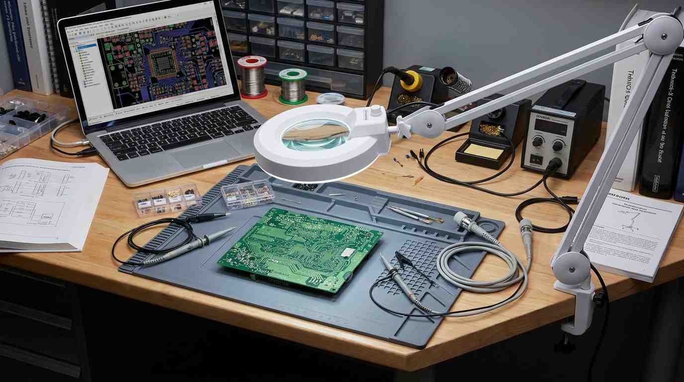
Short answer: Choose a CPLD-class device when the design demands instant-on, deterministic, low-complexity supervisory or glue logic. Choose an FPGA when the design demands high-density parallel compute, embedded DSP/MAC throughput, rich memory buffering, and high-speed serial connectivity. The decision hinges less on raw speed and more on configuration volatility, timing determinism, power architecture, board-level BOM overhead, and modern lifecycle reality.Executive Summary & Quick Engineering Decision FrameworkHardware designers comparing CPLDs and FPGAs have traditionally encountered a simple density-versus-determinism trade-off. A Complex Programmable Logic Device historically implemented modest logic functions through coarse-grained macrocells with deterministic timing and single-supply board requirements. A Field-Programmable Gate Array provided far greater logic capacity and dedicated arithmetic blocks at the cost of volatile configuration, multi-rail power sequencing, and place-and-route timing complexity.That architectural distinction remains useful, but it is no longer sufficient. Many classic pure macrocell CPLDs are end-of-life or not recommended for new designs, while modern single-chip Flash-based micro-FPGAs now fill the instant-on supervisory role. The selection question has therefore shifted: which programmable-logic architecture minimizes system-level risk while satisfying capacity, timing, and power constraints?Architectural Comparison MatrixComparison ParameterClassic CPLD / Flash-PLD ClassFull-Featured SRAM FPGAModern Single-Chip Flash FPGALogic fabricMacrocell / AND-OR product-term arraysConfigurable Logic Blocks (CLBs) with distributed LUTsLUT-based fabric with on-chip non-volatile configuration memoryConfiguration volatilityNon-volatile internal Flash/EEPROMVolatile SRAM; requires external boot FlashNon-volatile on-chip FlashPower-on latencyInstant-on (microsecond regime)Bitstream boot transfer (milliseconds to seconds)Sub-millisecond to near-instant-onTiming behaviorDeterministic, uniform pin-to-pin propagation delayPlace-and-route dependent; requires iterative timing closurePredictable, though routing-dependent within a single chipDedicated hard IPMinimal or noneDSP slices, Block RAM, PLLs, high-speed SerDesVaries by family; some include PLLs, ADC, and embedded Flash memoryPower architectureSingle-supply or simple dual-rail, low quiescentMulti-rail core/aux/IO PMIC sequencing, higher static leakageSingle-supply or simplified multi-railTypical logic capacityTens to hundreds of macrocellsThousands to millions of LUTs / Logic ElementsHundreds to tens of thousands of LUTsPrimary application fitPower sequencing, bus bridging, interrupt management, glue logicVideo processing, software-defined radio, networking, AI accelerationBoard management, secure boot, mixed-signal supervisionSilicon Selection Rule of ThumbUse this sequence before committing to any device family:Estimate true logic capacity. If the design needs more than roughly a few thousand flip-flops, a classic macrocell CPLD will likely fail capacity.Identify the cold-boot supervisor requirement. If no configured device can be safely released from reset until power rails are stable, an instant-on programmable-logic device must exist on the board.Inventory specialized hardware needs. Design sections requiring DSP MAC units, large Block RAM, or transceiver channels point directly to an FPGA.Audit the power sequencing architecture. A single-rail system tolerant to slow ramp behavior can accept a simpler device; a multi-rail SoC or high-density FPGA needs sequenced enable control.Check the vendor lifecycle status for every candidate part before schematic freeze. Do not rely on legacy CPLD families still appearing in old application notes or distributor search results.Silicon Fabric Architecture: Coarse Macrocells vs. Fine-Grained Look-Up TablesThe CPLD Logic StructureClassic CPLDs descend directly from programmable array logic and programmable logic arrays tracing back to the PAL/PLA era. The internal fabric is built around wide AND-OR product-term arrays feeding configurable macrocells. Each macrocell typically contains a flip-flop, polarity control, and feedback paths into the centralized interconnect matrix.This architecture is optimized for wide fan-in boolean equations. A 32-input address decode, for example, can be evaluated in a single uniform macrocell cycle without passing through multiple cascaded LUT stages. The wide product-term structure is the reason CPLDs have historically been favored for address decoding, bus arbitration, interrupt merging, and state machines with modest sequential depth[1].The limitation is equally architectural. Product-term resources are coarse and consumed inefficiently by arithmetic-heavy logic such as multipliers, barrel shifters, or wide addition trees. Attempting to build a 32-bit multiply-accumulate path inside a macrocell fabric quickly exhausts available product-term budget and yields poor performance.The FPGA Logic StructureFPGAs use an island-style architecture built around fine-grained Configurable Logic Blocks. Each CLB contains multiple Look-Up Tables, commonly with four or six inputs, paired with dedicated storage elements and local routing multiplexers. The LUT truth-table implementation supports arbitrary combinational logic within the LUT's input width; wider logic is decomposed across multiple cascaded LUTs connected through segmented routing channels.This fine-grained fabric scales far more gracefully for complex sequential state machines, deeply pipelined arithmetic datapaths, and dense parallel processing. The presence of dedicated carry chains, synchronous reset networks, and hierarchical clock distribution enables high-frequency datapath implementations that would be impractical in a coarse macrocell fabric.The trade-off is routing complexity. The segmentation of the FPGA interconnect means intermediate signals travel through programmable switch matrices whose electrical parasitics depend on placement and routing congestion. That reality gives rise to the timing-closure burden discussed in a later section.Architectural Trade-OffArchitectureStrengthsWeaknessesMacrocell product-termWide fan-in decoding, uniform delay, simple timing modelCoarse granularity, poor arithmetic efficiency, limited embedded IPLUT/CLB fabricFine granularity, excellent arithmetic and datapath scaling, integrated DSP/BRAMRouting-dependent delay, timing closure effort, larger fabric overheadComparison of coarse CPLD fabric versus fine-grained FPGA fabricConfiguration Memory, Volatility, and the "First-to-Wake" Power Sequencing ImperativeConfiguration Storage MechanismsThe divergence in configuration memory is one of the most consequential differences between CPLD-class devices and SRAM FPGAs.A classic CPLD stores its logic configuration in internal non-volatile EEPROM or Flash. The device wakes immediately once the supply rail stabilizes. There is no external configuration clock, no bitstream interface, and no boot memory component.A conventional SRAM-based FPGA stores its logic configuration in volatile SRAM latches that lose state at power-down. The configuration bitstream resides in an external SPI NOR Flash or QSPI memory and must be streamed into the FPGA on every power cycle. That process consumes milliseconds to seconds depending on bitstream size and configuration interface speed.The "First-to-Wake" Hardware ImperativeThe engineering consequence is deceptively simple: a volatile FPGA or complex SoC cannot manage its own power-up sequence. Before configuration is loaded, the FPGA's I/O pins are undefined and its internal fabric cannot run the power-rail sequencing state machine needed to safely bring up the board.This is where the CPLD-class device earns its place on the modern PCB. Acting as a board-management controller, an instant-on programmable-logic device can:Assert enable signals to PMIC regulators in the correct orderMonitor power-good flags from each railEnforce monotonic voltage ramp behaviorHold the main processor or FPGA in reset until all supplies are stable and the system clock is validDeassert reset and release the main compute device only after Boot-up requirements are satisfiedETH Zurich research on declarative power sequencing using CPLDs demonstrates this precise application[5]: deterministic state-machine control over power-rail enable and reset scheduling in complex compute platforms.Hardware Security and IP ProtectionConfiguration storage architecture also has direct security implications. An SRAM FPGA's bitstream travels over an exposed board-level SPI or QSPI bus, creating a point where the configuration image can be passively sniffed or actively manipulated. Modern SRAM FPGAs mitigate this through bitstream encryption and authentication keys, but the attack surface remains.A CPLD or Flash-based PLD stores configuration entirely on-chip, with no external boot bitstream to intercept. The non-volatile configuration memory is a security-relevant feature in systems requiring IP protection or resilient boot behavior.Verified Modern Instant-On ExampleThe Lattice MachXO3 family demonstrates the modern Flash-PLD approach: per the Lattice MachXO3 datasheet, sub-1 ms wake-up directly from on-chip non-volatile Flash across densities from 640 to 9,400 LUTs and up to 384 I/O pins. Similarly, per the Intel MAX 10 device overview, Intel MAX 10 single-chip FPGAs integrate on-die Configuration Flash Memory and offer dedicated Instant-On modes requiring supply ramp rates within 3 ms to wake without external boot bitstream latency.These specifications matter because they prove the CPLD-style instant-on role is being fulfilled by modern Flash-based single-chip architectures rather than legacy macrocell parts.Timing Determinism & Routing: Continuous Interconnects vs. Place-and-Route ComplexityCPLD Timing PredictabilityClassic CPLDs use a centralized, continuous routing matrix that connects all macrocell outputs and inputs through fixed-length interconnect paths. This topology produces a uniform pin-to-pin propagation delay that is largely independent of where a particular logic function is physically placed within the device.The engineering benefit is timing predictability. An asynchronous address decoder, a reset-merge circuit, or a bus bridge built in a CPLD exhibits consistent delay characteristics across the full operating temperature and voltage range. There are no routing congestion surprises because the routing matrix is not segmented.FPGA Routing RealitiesFPGAs replace the continuous interconnect with segmented routing channels and programmable switch matrices. Signals travel across variable lengths of metal interconnect, pass through multiple switch boxes, and suffer RC delay contributions that depend on physical placement and the degree of routing congestion in the critical path.Consequently, FPGA timing cannot be accurately predicted during schematic design. Engineers must run iterative Static Timing Analysis, apply physical synthesis constraints, and repeatedly place-and-route the design to close timing. A critical path that meets timing at 90% utilization may fail at 95% utilization when routing resources become scarce.Engineering ImpactThe timing-determinism difference has direct consequences for design verification. A hard real-time bus bridge in a CPLD requires fewer simulation cycles and fewer board-level re-spins because the timing model is fixed by architecture. The same function implemented in an FPGA demands careful constraint definition, timing-closure iterations, and re-verification after every logic change.Timing AttributeCPLD-Class DeviceSRAM FPGADelay modelDeterministic, uniformRouting-dependent, variableTiming predictionAvailable at schematic stageRequires post-PnR analysisRace condition risk in async logicLowElevated without careful constraintVerification burdenLowSignificant iterative STAPower Dissipation Dynamics: Quiescent Leakage vs. High-Speed Dynamic SwitchingMathematical Power ModelTotal power consumption in CMOS programmable logic follows the standard formulation:Ptotal=Pstatic+PdynamicPdynamic=CPD·VCC2·f·NSWwhere CPD is power dissipation capacitance, VCC is the core supply voltage, f is the switching frequency, and NSW is the number of switching nodes.Static Power and Quiescent OverheadThe static component is where SRAM FPGAs and CPLD-class devices diverge sharply. An SRAM FPGA must maintain configuration state in thousands or millions of SRAM cells even when no useful logic is switching. High-speed transceiver bias circuits, PLL analog blocks, and configuration control logic all draw quiescent current. This baseline static leakage exists independent of user design activity.Low-density CPLDs and Flash-PLDs, by contrast, can enter extremely low quiescent states because their non-volatile configuration memory does not require continuous latch power to retain state. When the design demands a wake-up supervisor that stays powered during system sleep, this low-standby characteristic is directly relevant.Dynamic Power Scaling Under Clock LoadDynamic power is where simplistic comparisons between CPLDs and FPGAs break down. A CPLD toggling wide product-term arrays at high frequency draws substantial dynamic current because wide internal nodes swing simultaneously across the routing matrix. A large SRAM FPGA toggling only a small portion of its fabric may dissipate less dynamic power than expected, but its static leakage remains present regardless of utilization.The practical implication: architectural power claims are meaningless without specifying clock frequency, toggle rate, logic utilization, and supply voltage. Use vendor power estimation tools and application notes to calculate device-specific thermal budgets before making a selection decision.Power scaling: CPLD static leakage versus FPGA dynamic switchingTotal Cost of Ownership & PCB Complexity: The Hidden BOM Overhead of FPGAsBeyond Silicon CostComparing bare silicon prices between a CPLD and an entry-level FPGA is misleading because the supporting component bill-of-materials differs dramatically.BOM FactorCPLD-Class DeviceSRAM FPGAConfiguration memoryNone requiredExternal SPI/QSPI NOR FlashPower suppliesSingle-rail or simple dual-railMulti-rail: core, I/O, aux, possibly transceiver railPower management ICDiscrete LDO or simple regulatorMulti-output PMIC with sequencingClockingSimple crystal or RC oscillatorLow-jitter differential oscillator often required for transceiversDecouplingBasic decoupling per I/O bankHigh-frequency capacitor arrays across multiple railsPCB layer count2–4 layers feasible6–12+ layers common for BGA fanoutPackage mountingHand-solderable QFP/QFN/TSSOPFine-pitch BGA requiring reflow and possible HDIPCB Fabrication and Layout ConstraintsClassic CPLDs and small Flash-PLDs are frequently available in low-pin-count, hand-solderable packages well suited to 2- to 4-layer PCBs. This simplifies prototyping and low-volume production.SRAM FPGAs, especially mid-range and high-density families, are packaged in fine-pitch BGAs that require high-layer-count stackups, controlled-impedance routing, and sometimes blind/buried microvias for breakout. The result is higher fabrication cost, longer layout cycles, and more complex design reviews.Package TypeTypical Pin CountPCB ImplicationsCPLD QFP/QFN44–144 pins2–4 layer PCB feasible, manual rework possibleFPGA Fine-Pitch BGA256–1,760+ balls6–12+ layer PCB, HDI routing, reflow-only assemblyThe Modern Supply Chain Reality: CPLD Obsolescence vs. Single-Chip Flash FPGAsWhy Legacy Guides and Current Answers DisagreeEngineers researching CPLD vs FPGA today encounter conflicting information. Some older application notes and tutorials still recommend classic 5V or 3.3V macrocell CPLD families that are no longer viable for new designs. Meanwhile, procurement catalogs increasingly use the term "CPLD" to refer to single-chip Flash-based micro-FPGAs with LUT fabrics.This lifecycle gap is not merely academic. Designing a legacy macrocell CPLD into a long-lifecycle industrial, defense, or medical product carries direct supply-chain risk.The Verified Lifecycle RealityAMD issued Product Discontinuation Notice XCN23009, dated January 1, 2024, with a final Last Time Buy on June 29, 2024. That notice officially terminates pure macrocell CPLD families including the XC9500XL, CoolRunner XPLA 3, and CoolRunner II lines, as well as legacy Spartan-II and Spartan-3 FPGAs, with no direct drop-in replacements.This notice provides concrete evidence for a broader industry pattern: the pure AND-OR macrocell CPLD architecture has largely exited mainstream production. Engineers evaluating "CPLD vs FPGA" must therefore distinguish between historical macrocell parts and modern single-chip Flash programmable devices marketed under similar names.The Rise of Modern Single-Chip Flash-Based Micro-FPGAsThe practical replacement for legacy macrocell CPLDs is the modern single-chip Flash micro-FPGA. Families such as Intel MAX 10, Lattice MachXO2/MachXO3/MachXO5, and Microchip IGLOO2 combine non-volatile on-chip configuration memory with instant-on microsecond boot, single-supply operation, and flexible LUT-based logic fabrics.These devices are not merely shrunk FPGAs. Per the Intel MAX 10 device overview, the MAX 10 family specifically integrates on-die Configuration Flash Memory and 12-bit 1 MSPS SAR ADCs, allowing a single chip to wake immediately, supervise power rails, and monitor analog telemetry without an external boot PROM. The MachXO3 family, as noted earlier, achieves sub-1 ms instant-on across up to 9,400 LUTs per the Lattice MachXO3 datasheet.Practical Migration GuidanceWhen updating a legacy design or starting a new hardware revision:Search for lifecycle status by exact part number, not by architecture family name.Treat every legacy CPLD appearing in an old schematic as a redesign candidate.Evaluate Flash micro-FPGA families for both capacity and instant-on suitability.Do not assume a "CPLD" search result is an active macrocell product. Verify against the manufacturer's current product catalog and PCN history.Engineering Selection Framework: When to Choose Which ArchitectureOption A: CPLD-Class Device or Single-Chip Flash-PLDBest for: Board supervisory logic, multi-rail power sequencing, interface level-shifting, wide address decoding, bus arbitration, and hardware-enforced fail-safe functions.Key strengths:Microsecond cold-boot latency when system power stabilizesDeterministic pin-to-pin propagation delay for asynchronous control pathsMinimal BOM overhead: no external configuration memory requiredSimple 2–4 layer PCB layout with hand-solderable packagesNon-volatile on-chip configuration protects IP and prevents bitstream interceptionKey drawbacks:Limited logic density relative to FPGAs; macrocell fabrics in particular cannot scaleMinimal or no dedicated DSP blocks, Block RAM, or high-speed transceiversPoor efficiency for wide arithmetic, multipliers, or deeply pipelined datapathsWho should NOT choose this option: Designs requiring audio/video processing, large packet buffering, multi-gigabit SerDes, complex math acceleration, or dense parallel compute.Option B: Full-Featured SRAM FPGABest for: Digital Signal Processing, multi-gigabit networking, computer vision, software-defined radio, AI inference at the edge, and embedded soft-core or hard-core processor SoCs.Key strengths:Massive parallel compute capability and reconfigurable datapath pipeliningRich dedicated hard IP: DSP slices, Block RAM, PLLs/MMCMs, PCIe/Ethernet transceiversScalable logic capacity across multiple density tiersWide ecosystem of vendor synthesis and verification toolsKey drawbacks:Higher static leakage current due to large configuration latch arraysMillisecond-level boot latency requiring external SPI flashComplex multi-rail PMIC requirements with controlled sequencingLengthy timing closure cycles requiring iterative STAFine-pitch BGA packages driving high-layer-count PCB designsWho should NOT choose this option: Designs needing simple reset sequencing, discrete GPIO expansion, low-cost single-rail battery operation, or minimal board complexity.Alternative Silicon Boundary AnalysisProgrammable logic is not always the right answer. Two adjacent technologies deserve explicit consideration.Ultra-low-power MCU. When the control path is inherently sequential and execution latencies in the microsecond range are acceptable, a small MCU may provide equivalent system supervision at lower cost and lower active power. The MCU's interrupt latency and software boot time must be carefully verified against the system's power-sequencing requirements.Configurable mixed-signal ICs. For very simple glue logic, analog comparator monitoring, and basic power-sequencing tasks, devices such as the Renesas GreenPAK SLG46826 offer an alternative. Per the Renesas SLG46826 datasheet, the SLG46826 provides dual-rail voltage translation supporting VDD from 2.3 V to 5.5 V and VDD2 from 1.71 V to 5.5 V, four rail-to-rail analog comparators, and programmable delay macrocells in a 2.0 mm × 2.2 mm 14-pin STQFN package. When the logic requirement fits within this class of device, the BOM overhead and board space can be substantially lower than even a small CPLD.Common Hardware Selection MistakesOver-specifying an FPGA for simple GPIO expansion — The result is unnecessary layout complexity, multi-rail power sequencing burden, and a larger PCB stackup.Under-specifying a CPLD for math-heavy state machines — Wide arithmetic and multiplier functions exhaust macrocell product-term resources rapidly.Ignoring cold-boot timing gaps — A design that releases the main processor from reset before power-good confirmation can exhibit destructive latch-up or intermittent boot failures.Assuming legacy CPLD availability — Failure to verify lifecycle status results in parts that become unobtainium mid-design.Treating bare silicon cost as total cost — A low-cost FPGA that requires a $6 PMIC, external flash, and a 10-layer PCB may cost more at the board level than a single-supply CPLD.Frequently Asked QuestionsAre pure macrocell CPLDs still being manufactured for new designs?Most pure AND-OR macrocell lines are legacy, NRND, or EOL. AMD's Product Discontinuation Notice XCN23009 (2024) officially terminated the XC9500XL, CoolRunner XPLA 3, and CoolRunner II families with a final Last Time Buy of June 29, 2024. New commercial designs primarily use Flash-based single-chip micro-FPGAs that provide instant-on, single-chip operation using modern LUT fabrics. Always verify lifecycle status against the manufacturer's current product catalog.Can an FPGA directly replace a CPLD on an existing PCB?Rarely as a drop-in replacement. SRAM FPGAs generally require different package pinouts, additional core voltage rails, and external configuration memory. A Flash-based micro-FPGA may come closer functionally, but package and electrical incompatibilities typically require a board revision. Any replacement candidate must be validated against the original schematic's voltage domains, pin mapping, and timing constraints.What are the primary technical disadvantages of pure CPLDs?The coarse macrocell granularity makes them inefficient for wide arithmetic and complex datapath processing. They also lack integrated Block RAM and DSP slices, which prevents execution of complex data processing pipelines. In addition, many classic macrocell families are no longer available for new designs.How does a CPLD differ from a fast microcontroller in control paths?CPLDs provide true hardware-level concurrency with nanosecond-scale deterministic propagation delays. MCUs execute sequential software instructions with interrupt latencies in the microsecond range. A CPLD's parallel hardware responds to input changes without software overhead, making it suitable for combinatorial decode, asynchronous bus arbitration, and hardware-enforced fail-safe logic that cannot tolerate software boot time.Difference Between CPLD and FPGA | Programmable Logic Devices | Digital Electronics in EXTCHardware Engineering Verification Checklist Before Silicon ProcurementUse this checklist before freezing the schematic or signing the BOM.[ ] Power supply count and sequencing — Verify whether the device requires single-rail operation or multi-rail PMIC sequencing. Identify every enable, soft-start, and power-good input.[ ] Cold-boot startup latency — Confirm the exact time-to-active from voltage threshold to operational state. For Flash micro-FPGAs, verify the instant-on spec against the system's power-sequencing target.[ ] Propagation delay constraints — Confirm worst-case pin-to-pin delay across operating temperature and speed grades for asynchronous decode paths.[ ] I/O bank compatibility and hot-socketing — Verify voltage tolerance (1.2 V, 1.8 V, 2.5 V, 3.3 V), fail-safe clamps, and floating-pin behavior during power ramping.[ ] Vendor lifecycle status and PCN history — Verify active production status and review recent Product Change Notifications. For any legacy part, check for discontinuation notices before committing the design.[ ] Package fanout and PCB layer feasibility — Check package pitch (e.g., 0.5 mm BGA vs. 0.8 mm QFP) to confirm stackup layer count, via technology, and fabrication cost.[ ] Thermal envelope and static leakage — Calculate worst-case junction temperature based on maximum quiescent leakage and switching frequency. Use the vendor's power estimator if available.[Sources and references used for this guideCPLD - What is the difference between CPLDs and FPGAs?Source type: official company documentationUsed for: Canonical definitions of macrocell product-term architectures versus Look-Up Table (LUT) FPGA fabrics, non-volatile internal routing, and configuration memory distinctions.Caution: Vendor support documentation representing AMD/Xilinx architectural classifications; focus on structural silicon mechanisms rather than specific legacy part recommendations.Hot-Socketing & Power-Sequencing Feature & Testing for Altera DevicesSource type: official company documentationUsed for: Technical analysis of PLD power-up sequencing, hot-socketing capabilities, I/O pin behaviors during supply ramping, and hardware supervisory roles.Caution: Official Altera/Intel technical collateral; focuses on device reliability and power behavior rather than third-party competitive comparisons.Power-Aware FPGA DesignSource type: official company documentationUsed for: Modeling static leakage current, dynamic switching dissipation, clock gating, and power optimization strategies across programmable logic fabrics.Caution: Vendor whitepaper emphasizing Microchip's Flash-based FPGA efficiency; calculations apply broadly to CMOS logic but narrative highlights proprietary low-power advantages.CMOS Power Consumption and CPD CalculationSource type: official company documentationUsed for: Mathematical modeling of CMOS dynamic power consumption, internal capacitance calculation, and frequency-dependent power scaling.Caution: Foundational semiconductor physics application note; establishes universal formulas (CV2f) rather than programmable device selection heuristics.Declarative Power Sequencing using a CPLDSource type: research sourceUsed for: Academic and experimental validation of CPLD deterministic timing in real-time power supply rail sequencing and fault management in complex compute platforms.Caution: Academic research paper focused on specific power management implementations; demonstrates determinism advantages but does not cover general-purpose FPGA compute workloads.Models for reducing power consumption in CPLD and FPGA devicesSource type: research sourceUsed for: Comparative academic study on static leakage versus dynamic power dissipation under varying clock frequencies in programmable logic.Caution: Conference paper; provides comparative modeling data but utilizes specific older generation test benches.CPLD vs FPGA: Key Differences and How to ChooseSource type: reputable professional sourceUsed for: Engineering overview of macrocell vs LUT density, pin-to-pin propagation delay differences, and high-level selection criteria.Caution: Tertiary engineering publication; serves as a structuring reference for design trade-offs, but specific numerical figures must be cross-checked against component datasheets.GreenPAK vs FPGA vs CPLD: Which Is Right for Your Design?Source type: vendor articleUsed for: Board-level PCB design trade-offs, package footprints, and boundary comparisons between programmable logic, microcontrollers, and mixed-signal arrays.Caution: EDA vendor blog; useful for PCB layout and routing perspective, but contains commercial product references.
On 2026-08-25