 info@kynix.com
 00852-6915 1330


 0
0


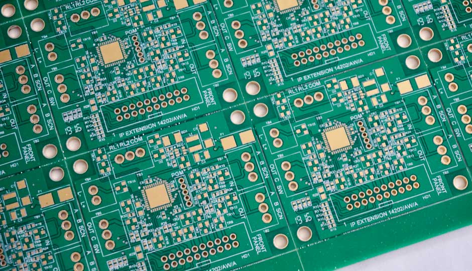
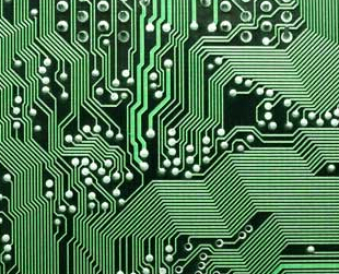
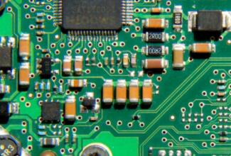
ⅠIntroductionAs electronic technology advances, there is a greater need for high-speed PCB design. Because they can work at high speeds with integrated circuits for most electronic devices, even simple ones. Some factors and parameters have to be considered when designing a high-speed PCB. Furthermore, you will discover that the fundamental PCB design rules and methods you have mastered are exactly what you need to learn. Needless to say, it will be extremely useful to PCB designers working on high-speed PCB designs.CatalogⅠIntroductionⅡ What is High-speed PCB Design?Ⅲ High-speed PCB Related VideoⅣ When Is a Printed Circuit Board Design Considered High Speed?Ⅴ High-speed PCB Design SkillsⅥ High speed PCB Design ConsiderationsⅦ Setup for High-Speed DesignⅧ Floorplanning a High Speed PCBⅨ How to Tell If Your Project is High SpeedⅩFAQ Ⅱ What is High-speed PCB Design?High-speed PCB design is any design in which the physical characteristics of your PCB. such as layout, packaging, interconnection, layer stack up, and so on, begin to impact the integrity of your signals. Furthermore, when you begin designing the boards and encounter issues such as delays, crosstalk, reflections, or emissions, you will enter the world of high-speed PCB design, Because of the attention paid to these issues, high-speed design is truly unique. You may be accustomed to designing a simple PCB where you focus primarily on component placement and routing. However, it is more important to consider some factors when using a high-speed design, such as how close they are to signals, what width they will be, where you will place the traces, and what types of components they will be connected to. Furthermore, when the factors are considered, it will achieve a high level for your PCB design process.Figure1:What is High-speed PCB Design? Ⅲ High-speed PCB Related Video High-Speed PCB Design Tips - Phil's Lab #25 High-speed PCB Video Description: Quick overview of some general high-speed PCB design tips. Everything from stack-ups, controlled impedance traces, vias, and much more! Ⅳ When Is a Printed Circuit Board Design Considered High Speed?Certain characteristics can help you identify a high-speed PCB design, As a result, the design is fast if:It uses HDMI , Ethernet, SATA , PCI Express, USB, Thunderbolt, or other high-speed interfaces for fast data transfer; the circuit consists of several sub-circuits connected via high-speed interfaces (LVDS, DSI, CSI, SDIO, DDR3 , etc.); the time of signal propagation over the track is at least 13 of the time of signal rise; the digital signal frequency is 50MHz or higher;Because the printed circuit board is so small, locating the components becomes a real challenge (especially when you come across a high-speed interface layout ). Ⅴ High-speed PCB Design SkillsBe familiar with design software that provides advanced options.High-speed designs necessitate a plethora of complex features in your CAD software. Furthermore, there may not be many programs for hobbyists, and it rarely has advanced options based on Web suites. As a result, you must gain a better understanding of a powerful.High-speed routing When it comes to high-speed traces. a designer needs to understand the essential routing rules, such as not cutting ground planes and keeping trails short. As a result, keep digital lines a certain distance apart from crosstalk and shield any interference-creating elements from compromising signal integrity.Routing traces with impedance controlImpedance matching is required for some types of signals with impedances ranging from 40 to 120 ohms. Antennae and a large number of differential pairs are examples of characteristic impedance matched hints.It is critical for designers to understand how to calculate trace width and layer stack for required impedance values. If the impedance values are incorrect, it can have a serious impact on the signal, resulting in data corruption. When creating a PCB layout or a high-speed PCB layout. keep single-ended impedance Zo and differential impedance Zdiff in mind. Figure2: Parameters for Zdiff calculation Length matching traces High-speed memory buses and interface buses have numerous lines. Because the lines can operate at high frequencies, it is critical that the signals travel from the transmitting terminal to the receiving terminal at the same time. Furthermore, it must have a feature known as length matching. As a result, most common standards define tolerance values that must match length.Figure3: High-speed PCB Design SkillsMinimizing loop areaHigh-frequency signals can cause EMI and EMC issues, so high-speed PCB designers should be aware of these tips. As a result, they must follow basic rules such as having continuous ground planes, reducing loop areas by optimizing current return paths for traces. and incorporating numerous stitching vias. Ⅵ High speed PCB Design ConsiderationsThe importance of the PCB layout cannot be overstated.PCB Design ConsiderationsSchematic considerationsTrace length tuningPCB materials and stack-up demands for high speedHigh-speed placement strategiesDifferential pair and trace length routing Crosstalk, impedance control, and parallelism considerationsUnderstanding stripline and microstripRouting topologies and best routing practicesSimulators Ⅶ Setup for High-Speed DesignBefore the layout can begin, there are several design and database details that have to be addressed.SchematicWhile there is a lot to set up before you can start the layout of a high-speed design, most people don't give the schematic much thought. Designers need to check the parts, simulate the circuitry, and finish the design. Is the schematic, however, ready to be used for layout? If the designer cannot easily understand the intent of the circuitry, an unorganized schematic can make the PCB layout difficult. High-speed signal paths, for example, must be laid out sequentially so that the designer can replicate component placement in the layout, It's also a good idea to highlight parts of the design that you really understand.These include:Critical placement locations, as well as which side of the board certain parts may be required onKeep out zones should be established around critical components.High-speed routing data, such as topologies, measured lengths, and matched lengths.Information about a differential pair and controlled impedance. PCB LibrariesAs with any PCB layout. the component footprints used for high-speed design must be checked and verified, but some additional library work may be required. Some footprints used in high-frequency or RF designs, for example, may require modifications to reduce pad sizes for signal integrity, In addition, to accommodate high-density design requirements, some footprints may be reduced to their smallest size. However, component footprints should always adhere to industry and manufacturer specifications to the greatest extent possible to meet design for manufacturability (DFM) requirements. Many design tools, including Cadence's Allegro PCB Editor, include online library browsing capabilities for importing vendor-specific footprint models. Materials and ComponentsBefore you begin the layout. you must choose the materials that will be used to construct your high-speed circuit board. Harsh operating environments may necessitate a more robust board structure, and the physical properties of the materials will be required for calculated controlled impedance routing :Consult with your manufacturer to determine whether your board will require high-speed materials.For high-speed and high-frequency applications, enhanced epoxy or PTFE materials may be a better choice.The dielectric constants of FR-4 may be insufficient to hold the impedance values required, or the design may suffer from greater signal loss than is acceptable.The manufacturer will also need to review and confirm the PCB components. With today's supply chain issues, you'll want to make sure you have enough parts before committing to a design. Board Layer StackupSpecific board layer stack-ups are required for high-speed designs to aid in EMI shielding and signal integrity, The primary concern is to include a complete and continuous ground plane on an internal layer. Many boards will also have multiple ground plane layers spread across the board stack up to accommodate multiple layers of transmission line routing in microstrip or stripline configurations. The board layer stack-up must be created in the PCB CAD database or imported from another source. This is where the ability of PCB design systems to communicate directly with the vendor for stack-up information exchange, as demonstrated in the video above, can be extremely useful. Design RulesPCB design systems typically include a comprehensive set of design rules and constraints that can be applied to the design. Component and net classes will already be used in standard circuit board designs to specify spacing rules, trace widths, vias, and other constraints. With a high-speed design, a completely new set of rules should be established, including:Differential pairsSignal pathsRouting topologiesMeasured and matched trace lengthsTrace tuning parameters These rules can be set up for each design, or in many cases, imported from another layout to ease the designer’s workload. System ParametersThe parameters are the last but not least of the setups. Display parameters such as colors and fill patterns, grids, routing preferences, and a slew of others are among them. Designers can improve their tool efficiency by managing these parameters, Let's start laying out the board now that we've completed the high-speed design.Figure5: A PCB CAD system’s parameter setup menu for design colors Ⅷ Floorplanning a High Speed PCBIn a high-speed PCB layout , there are no specific rules or standards for where components should be placed. In general, the largest central processor IC should be placed near the center of the board because it will typically need to interface with all other components on the board in some way. Smaller integrated circuits (ICs) that connect directly to the central processor can be placed around the central IC to keep routing between components short and direct. Peripherals can then be added to the board to provide the necessary functionality.When the main controller IC is near the center of the board, and other high-speed peripherals are placed around it, the high-speed layout works best. This is one of the reasons why motherboards have a large processor in the center of the board. The Altium Designer MiniPC project has its PCIe, DDR4, USB 3.0, and Ethernet peripherals arranged around the central FPGA SoC to facilitate routing.Figure6: high-speed PCB layoutOnce your components are in place, you can use your design tools to begin routing your design. This is a critical aspect of high-speed board design because incorrect routing can compromise signal integrity. However, if the preceding steps were followed correctly, signal integrity is much easier to achieve. Set your impedance profile in your PCB design rules so that all routers in the design have the proper width, clearance, and spacing to maintain controlled impedance during routing. Ⅸ How to Tell If Your Project is High SpeedThere are a couple of schools of thought on this. The unfortunate reality is that there is no specific definition of what constitutes a high-speed PCB. It all comes down to a case-by-case assessment. As previously stated, if you're experiencing signal integrity issues on your PCB layout. it's a good indication that you're working on a high-speed project.There's also the device-specific approach to consider. You'll be working on a high-speed project if you're designing a motherboard, cell phone board, or DSL router board. If you need to incorporate specific technologies into your layouts, such as HDMI, PCI Express, USB, or SATA, be aware that you will be dealing with high-speed design constraints.Figure7: Do you believe your design has a lot of traces? Take a look at this high-speed layout The final point to consider is whether you're working on a design with lumped or distributed circuits. What's the distinction? Designs with physical systems that are all small enough that they interact uniformly are referred to as lumped systems and are not fast. However, if your systems all operate independently within the confines of a larger whole, you have a distributed system and some high-speed design issues to deal with.Here is what you should remember:When the trace length becomes a significant fraction of the wavelength of the fastest signal, high-speed design considerations need to be considered.ⅩFAQ1. What is considered high speed design?High speed design specifically refers to systems that use high speed digital signals to pass data between components. The dividing line between a high speed digital design and a simple circuit board with slower digital protocols is blurry.2. What is high speed design Altium?High-Speed Design in Altium Designer. High-speed printed circuit board design is a process of balancing the circuit design requirements, device technologies, and fabrication materials and methodologies, to deliver a PCB that can transfer signals between the components, with integrity.3. What are high speed interfaces?High-Speed Serial Interface (HSSI) is a short-distance (50') communications interface that is used to interconnect routing and switching devices on slower local-area networks (LANs) with the higher-speed lines of a wide area network (WAN).4. What is high frequency PCB?High Frequency PCB is a type of PCB which is widely used in applications involving special signal transmission between objects. It is available in frequency range of 500MHz to 2GHz and is an ideal choice for mobile, microwave, radio frequency and high speed design applications.5. What is high speed signal in PCB?What is a high-speed signal in a PCB? Signals with frequencies ranging from 50 MHz to as high as 3 GHz are considered high-speed signals such as clock signals. Ideally, a clock signal is a square wave, but it is practically impossible to change its 'LOW' level to 'HIGH' level (and vice versa) instantly.
On 2021-12-31


-PCB-Basics.html&media=https://static.kynix.com/imgs/BlogImage/ky_bg_head_20181222114545.jpg&description=What Is PCB(Printed Circuit Board) ? PCB Basics)