Catalog
| Overview |
|
|
| Structure and Working Principle of Power MOSFET | Structure of Power MOSFET |
|
| WorkingPrinciple of Power MOSFET |
|
| Basic Characteristics of Power MOSFET | Static Properties |
| Dynamic Characteristics |
| Switching Speed of MOSFET |
| Improvement of Dynamic Performance |
|
| Principle and Performance Analysis of High Voltage MOSFET |
Principle and Method of Reducing on Resistance of High Voltage MOSFET | On-Resistance Distribution of MOSFET with Different Voltage Resistance |
| The Idea of Reducing the On-Resistance of High Voltage MOSFET |
| Main Characteristics of Built-In Transverse Electric Field MOSFET | The Decrease of On-Resistance |
| The Reduction of Package and the Reduction of Thermal Resistance |
| Improvement of Switching Characteristics |
| Anti-Avalanche Breakdown Ability and SCSOA |
| Development Status of Built-in Transverse Electric Field High Voltage MOSFET |
|
| Comparison Between COOLMOS and IGBT |
|
| Power MOSFET Drive Circuit | Introduction and Analysis of Several MOSFET Drive Circuits | An Unisolated Complementary Drive Circuit |
| Isolated Drive Circuit |
1. Overview
The original meaning of MOSFET is Metal-Oxide-Semiconductor Field-Effect-Transistor. MOS means that the gate of the metal layer (M) is separated by the oxide layer (O) to control the field effect transistor of the semiconductor (S) by the effect of electric field.
Power field effect transistors are divided into junction type and insulated gate type, but it usually refers to the MOS type(Metal Oxide Semiconductor FET) in the insulation grid type, which is referred to as power MOSFET. Junction power field effect transistors are generally referred to as Static Induction Transistor (SIT). It is characterized in that the gate voltage is used to control the drain current, the drive circuit is simple, the drive power is small, the switching speed is fast, the working frequency is high, and the thermal stability is better than that of GTR. However, its current capacity is small and it can just withstand low voltage. Generally speaking, it is only suitable for power electronic devices whose power does not exceed 10kW.
2. Structure and working principle of Power MOSFET
Types of Power MOSFET:
According to the conductive channel, it can be divided into P channel and N channel.
According to the amplitude of gate voltage, it can be divided into: depletion type and enhancement type.
Power MOSFET is mainly N-channel enhancement type.
2.1 Structure of Power MOSFET
The internal structure and electrical symbols of the power MOSFET are shown in figure 1. When a monopole transistor is turned on, only one polar carrier (multiple carriers) is involved in the conduction. The conductive mechanism is the same as that of the low power MOSFET, but the structure is quite different. The low power MOSFET is a transverse conductive device. The power MOSFET mostly adopts the vertical conductive structure, also known as VMOSFET (Vertical MOSFET), which greatly improves the voltage and current resistance of MOSFET devices.

Fig 1.
According to the difference of vertical conductive structure, it can be divided into two types. One is VVMOSFET, which use V-shaped slot to achieve vertical conduction. Another is VDMOSFET (Vertical Double-diffused MOSFET), which has vertical conductive double diffusion MOS structure. In this article, VDMOS devices are discussed as an example.
The power MOSFET is a multivariate integrated structure, such as the hexagonal unit adopted by the HEXFET of International Rectifier, the square unit adopted by the SIPMOSFET of Siemens and rectangular unit adopted by TMOS of Motorola.
2.2 Working principle of Power MOSFET
Cut-off:
Positive power supply is added between drain and source, and the voltage between gate and source is zero. The J1 of the PN junction formed between the P base region P and the drift region N is inversely biased, and there is no current flow between the drain and source.
Conduction:
By adding a positive voltage UGS between the gate sources, the gate is insulated, so no gate current flows through it. However, the positive voltage of the gate pushes away the holes in the region P below it, and attracts the electrons, minority carrier in the region P to the surface of the region P below the gate.
When the UGS is greater than the UT (turn-on voltage or threshold voltage), the electron concentration on the surface of the region P under the gate will exceed the hole concentration, making the P-type semiconductor inverse into the N-type and become the inversion layer. The inversion layer forms the N channel and makes the PN junction J1 disappear. The drain and source conduct electricity.
2.3 Basic characteristics of Power MOSFET
2.3.1 Static properties: the transfer and output properties are shown in figure 2.
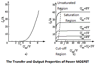
Fig 2.
The relationship between drain current ID and gate source voltage UGS is called the transfer characteristic of MOSFET. When the ID is large, the relationship between ID and UGS is approximately linear, and the slope of the curve is defined as transconductance Gfs.
The drain volt-ampere characteristics (output characteristics) of MOSFET are as follows:
Cutoff region (corresponding to the cutoff region of GTR)
Saturation region (corresponding to the magnification region of GTR)
Unsaturated region (corresponding to the saturation region of GTR)
The power MOSFET works in the switching state, which means that it switches back and forth between the cut-off zone and the unsaturated zone. There is a parasitic diode between the drain and source of power MOSFET, and the device is turned on when the reverse voltage is applied between the drain and source. The on-state resistance of power MOSFET has a positive temperature coefficient, which is beneficial to the current sharing of the devices connected in parallel.
2.3.2 Dynamic characteristics; the test circuit and switching process waveforms are shown in figure 3
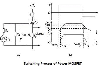
Fig 3.
2.3.3 Switching Speed of MOSFET
The switching speed of MOSFET has a lot to do with the charge and discharge of Cin. The user can not reduce the Cin, but can reduce the internal resistance of the drive circuit Rs, reduce the time constant and speeds up the switching speed. MOSFET only depends on multiple carriers to conduct electricity, and there is no minority carrier storage effect, so the turn-off process is very fast. The switching time is between 10-100ns, and the working frequency can reach more than 100kHz, which is the highest among the main power electronic devices.
When the field control device is static, there is little need for input current. However, during the process of switching, the input capacitor needs to be charged and discharged, and a certain amount of drive power is still needed. The higher the switching frequency, the greater the drive power required.
2.4 Improvement of dynamic performance
In the application of the device, in addition to considering the voltage, current and frequency of the device, we must also grasp how to protect the device in the application so as not to damage the device in the transient change. Of course, the thyristor is a combination of two bipolar transistors, coupled with the large capacitance brought by large area, so its dv/dt capability is relatively fragile. For di/dt, it also has a conduction zone extension problem, so it also brings quite strict restrictions.
The case of power MOSFET is very different. Its dv/dt and di/dt capabilities are often measured by its ability per nanosecond rather than per microsecond. But in spite of this, it also has the limitation of dynamic performance. These can be understood from the basic structure of power MOSFET.
Fig. 4 is the structure of the power MOSFET and its corresponding equivalent circuit. In addition to the fact that almost every part of the device has a capacitance, it must also be considered that the MOSFET is connected in parallel with a diode. At the same time, from a certain point of view, it also has a parasitic transistor, just as IGBT is parasitic on a thyristor. These aspects are very important factors to study the dynamic characteristics of MOSFET.
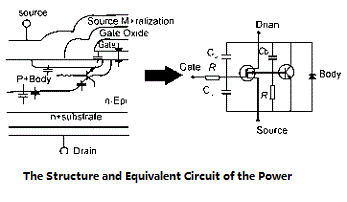
Fig 4.
First of all, the intrinsic diode attached to the MOSFET structure has certain avalanche ability. It is usually expressed as the ability of a single avalanche and the ability of repeated avalanche. When the reverse di/dt is very large, the diode will withstand a very fast pulse spike. It may enter the avalanche area, once its avalanche capacity is exceeded, the device may be damaged. As any kind of PN junction diode, it is very complex to study its dynamic characteristics carefully. They are very different from the simple concept that we generally understand that the PN junction is conducted when it is forward and blocked when it is backward. When the current drops rapidly, the diode loses its reverse blocking ability and this is the so-called backward recovery time. When the PN junction requires rapid conduction, there will be a period of time when the resistance is not very low. Once the diode has a positive injection in the power MOSFET, the injected minority carriers will also increase the complexity of the MOSFET as a multi-subdevice.
During the design process of power MOSFET, measures are taken to make the parasitic transistors as ineffective as possible. The measures are different in different generation of power MOSFET, but the general principle is to make the transverse resistance RB under the drain as small as possible. Because only when the transverse resistance under the region N of drain flows through enough current to establish the positive deviation condition for the region N, the parasitic bipolar thyristor begins to cause difficulties. However, under severe dynamic conditions, the transverse current caused by dv/dt through the corresponding capacitance may be large enough. At this point, the parasitic bipolar transistor will start, possibly causing damage to the MOSFET. Therefore, when considering the transient performance, attention must be paid to the internal capacitance of the power MOSFET device, which is the channel of the dv/dt.
The transient situation is closely related to the line condition, which should be paid enough attention in the application. In order to understand and analyze the corresponding problems, it is necessary to have an in-depth understanding of the device.
3. Principle and Performance Analysis of High Voltage MOSFET
In power semiconductor devices, MOSFET plays an important role in all kinds of power conversion, especially in high frequency power conversion with high speed, low switching loss and low drive loss. In the low voltage field, MOSFET has no competitors, but with the increase of the voltage resistance of MOS, the on-resistance increases to the power of 2.4 to 2.6. The growth rate makes MOSFET manufacturers and users have to reduce the rated current by tens of times in order to compromise the contradiction between rated current, on resistance and cost. Even so, the on-voltage drop caused by the on-resistance of the high-voltage MOSFET at the rated junction temperature is still high. The rated junction temperature and current of the MOSFET withstanding voltage above 500V are very high, and the on-voltage above 800V is astonishingly high. The conduction loss accounts for two-thirds to four-fifths of the total loss of MOSFET, which greatly limits the application.
3.1 Principle and Method of Reducing on Resistance of High Voltage MOSFET
3.1.1 On-resistance distribution of MOSFET with different voltage resistance:
The resistance proportional distribution of each part of the on-resistance of MOSFET with different voltage resistance is also different. For example, the epitaxial layer resistance of 30V MOSFET is only 29% of the total on resistance, and the epitaxial layer resistance of 600V MOSFET is 96.5% of the total on resistance. From this, it can be inferred that the on-resistance of 800V MOSFET will be almost occupied by the epitaxial layer resistance. In order to obtain high blocking voltage, the epitaxial layer with high resistivity must be used and thickened. This is the fundamental reason for the high on resistance caused by the conventional high voltage MOSFET structure.
3.1.2 The Idea of Reducing the On-Resistance of High Voltage MOSFET
Increasing the core area can reduce the on-resistance, but the cost is not allowed by commercial products. Although the introduction of minority carrier for conducting electricity can reduce the conduction voltage drop, but the price is the decrease of switching speed and the appearance of trailing current, the increase of switching loss and the loss of the high speed advantage of MOSFET.
The above two methods can not reduce the on-resistance of high voltage MOSFET, the remaining idea is how to separately solve the low doping of high voltage, high resistivity region and the high doping, low resistivity of conductive channel. For example, it has no other use except that the high voltage epitaxial layer low doping can only increase the on resistance. In this way, whether we can realize the conductive channel with high doping and low resistivity, and try to clamp the channel in some way when the MOSFET is turned off, so that the voltage withstand of the whole device depends only on the low doping N-epitaxial layer. Based on this idea, INFINEON introduced a built-in transverse electric field voltage of 600V COOLMOS in 1988 to realize this idea. The profile structure of the high voltage MOSFET with built-in transverse electric field and the schematic diagram of high blocking voltage and low on resistance are shown in figure 5.
Different from the conventional MOSFET structure, the MOSFET with the built-in transverse electric field embeds the vertical region P and clamps the region N of the vertical conductive region in the middle, so that when the MOSFET is turned off, the transverse electric field is established between the vertical P and N. The N doping concentration in the vertical conductive region is higher than that in the epitaxial region.
When VGS is less than VTH, the N-type conductive channel caused by the inversion of electric field cannot be formed, and the positive voltage between D and S makes the PN junction inside MOSFET backward bias to form a depletion layer and the vertically conductive region N is exhausted. This depletion layer has a longitudinal high blocking voltage, as shown in figure 5 (b), where the voltage resistance of the device depends on the voltage resistance of P and N-. Therefore, low doping and high resistivity of N-are necessary.
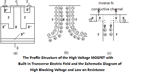
Fig 5.
When CGS is greater than VTH, the N-type conductive channel is formed by the inversion of electric field. The electrons in the source region enter the exhausted vertical region N to neutralize positive charge through the conductive channel, thereby restoring the exhausted N-type characteristics, so the conductive channel is formed. Because of the low resistivity in the vertical region N, the on-resistance will be significantly lower than that of the conventional MOSFET.
Through the above analysis, we can see that the blocking voltage and on-resistance are in different functional areas. The contradiction between the blocking voltage and the on-resistance is solved by separating the blocking voltage from the on-resistance function. At the same time, the surface PN junction is transformed into a buried PN junction, and the blocking voltage can be further increased at the same N-doping concentration.
3.2 Main Characteristics of Built-in Transverse Electric Field MOSFET
3.2.1 The decrease of on-resistance
The MOSFET of the built-in transverse electric field of the INFINEON withstands 600V and 800V respectively. Compared with conventional MOSFET devices, the on-resistance with the same core area decreases to one fifth and one tenth of conventional MOSFET, and the on-resistance decreases to one second and one third respectively at the same rated current. Under the conditions of rated junction temperature and rated current, the conduction voltage is reduced from 12.6V, 19.1V to 6.07V, 7.5V, and the conduction loss is reduced to one second and one third of conventional MOSFET, respectively. Because of the decrease of conduction loss, the decrease of heat and the relative coolness of the device, it is called COOLMOS.
3.2.2 The reduction of package and the reduction of thermal resistance
Compared with the conventional MOSFET, the core of the COOLMOS with the same rated current is reduced to one third and one fourth, which reduces the package by two shell specifications.
Because the thickness of COOLMOS core is only one third of that of conventional MOSFET, the RTHJC of TO-220 package is reduced from 1 ℃ / W to 0.6 ℃ / W, and the rated power is increased from 125W to 208W, which improves the heat dissipation capacity of the core.
3.2.3 Improvement of switching characteristics
The gate charge and switching parameters of COOLMOS are obviously better than those of conventional MOSFET. Due to the decrease of QG, especially QGD, the switching time of COOLMOS is about one second of that of conventional MOSFET, and the switching loss is reduced by about 50%. The decrease of turn-off time is also related to the low gate resistance in COOLMOS.
3.2.4 Anti-avalanche breakdown ability and SCSOA
At present, the new MOSFET has the ability to resist avalanche breakdown without exception. COOLMOS also has the ability to resist avalanche. At the same rated current, the IAS of COOLMOS is the same as ID25 ℃. However, because of the decrease of the core area, when the IAS is smaller than the conventional MOSFET, and has the same core area, the IAS and EAS are larger than the conventional MOSFET.
One of the biggest features of COOLMOS is that it has a short circuit safe operation area (SCSOA), but the conventional MOS does not have this feature. The SCSOA of COOLMOS is mainly due to the change of transfer characteristics and the decrease of core thermal resistance. The transfer characteristics of COOLMOS are shown in figure 6. As we can see from figure 6, when VGS is greater than 8V, the drain current of COOLMOS no longer increases, showing a constant current state. Especially when the junction temperature increases, the constant current value decreases, and at the highest junction temperature, it is about twice as much as ID25 ℃, that is, 3 to 3.5 times of the normal working current. In the short circuit state, the drain current will not rise to an intolerable ID25 ℃ due to the 15V drive voltage of the gate, so that the power dissipated by the COOLMOS in the short circuit is limited to 350V × 2ID25 ℃, so as to reduce the core heat during the short circuit as much as possible.
The decrease of the thermal resistance of the core can make the heat generated by the core radiate quickly to the shell and restrain the rising rate of the core temperature. Therefore, COOLMOS can be driven by normal gate voltage, withstand 10 MS short circuit shock under 0.6VDSS power supply voltage for 1000 times without damage and the time interval is greater than 1s. Therefore, COOLMOS can be protected effectively in short circuit like IGBT.

Fig 6.
3.3 Development Status of Built-in Transverse Electric Field High Voltage MOSFET
Following the introduction of COOLMOS in 1988, ST introduced 500V internal structure similar to COOLMOS in early 2000, so that 500V, 12A MOSFET can be packaged in TO-220 shell, the on-resistance is 0.35 Ω, which is lower than that of IRFP450, and the current rating is similar to that of IRFP450. IXYS also has MOSFET that uses COOLMOS technology. IR also introduced the super MOSFET, rated current of 35A and 59A in SUPPER220, SUPPER247 package, and the on-voltage drop of about 4.7V when the on-resistance is 0.082 Ω, 0.045 Ω and 150C, respectively. From the comprehensive index, these MOSFET are superior to the conventional MOSFET. The proportional decrease of on resistance is not due to the increase of core area. Therefore, it can be considered that the above MOSFET must have a special structure similar to the transverse electric field. It can be seen that trying to reduce the conduction pressure drop of high pressure MOSFET has become a reality, and will promote the application of high voltage MOSFET.
3.4 Comparison between COOLMOS and IGBT
The high temperature conduction voltage drop of 600V and 800V COOLMOS is about 6V and 7.5V respectively, the turn-off loss is reduced by one second, and the total loss is reduced by more than one second, so that the total loss is 40% to 50% of that of conventional MOSFET. The conduction loss of the conventional 600V MOSFET accounts for about 75% of the total loss, and the equilibrium point corresponding to the same total loss and ultra-high speed IGBT is 160KHZ, of which the switching loss accounts for about 75%. Because the total loss of COOLMOS is reduced to 40% to 50% of that of conventional MOSFET, the corresponding IGBT loss balance frequency will be reduced from 160KHZ to about 40KHZ, which increases the application of MOSFET in high voltage.
From the above discussion, it can be seen that the new high voltage MOSFET solves the problem of high conduction voltage drop, and can simplify the design of the whole machine, such as the volume of heat dissipation device can be reduced to about 40%, drive circuit and buffer circuit are simplified. It has the ability to resist avalanche breakdown and short circuit, simplify the protection circuit and improve the reliability of the whole machine.
4. Power MOSFET drive circuit
Power MOSFET is a voltage type driver. Because there is no minority carrier storage effect, the input impedance is high, the switching speed can be very high, the drive power is small, and the circuit is simple. However, the interpolar capacitance of the power MOSFET is large, and the relationship between the input capacitance CISS, the output capacitance COSS, the feedback capacitance CRSS and the interpolar capacitance can be expressed as follows:
The gate input of the power MOSFET is equivalent to a capacitive network, and its working speed is related to the internal impedance of the drive source. Due to the existence of CISS, the gate drive current is almost zero in static state, but a certain drive current is still needed in the dynamic process of turning on and off. It is assumed that the gate voltage required for saturation conduction of the switch tube is VGS, the turn-on time TON of the switch includes two parts: the turn-on delay time TD and the rise time TR.
During the turn-off process of the switch tube, CISS is discharged through ROFF, COSS is charged by RL, COSS is larger, VDS(T) rises slowly. With the increase of VDS(T), COSS decreases rapidly to close to zero, and VDS(T) increases rapidly.
According to the above analysis of the characteristics of the power MOSFET, the drive requirements are as follows:
The trigger pulse should have a fast enough rise and fall speed;
Charging with low resistance gate capacitance when turned on, and providing low resistance discharge circuit for gate when turned off in order to improve the switching speed of power MOSFET;
In order to enable the power MOSFET to turn on by trigger, the trigger pulse voltage should be higher than the opening voltage of the tube. In order to prevent misconduction, a negative gate source voltage should be provided at its cut-off time;
When the power switch switches, the drive current is the charge and discharge current of the gate capacitance. The larger the interelectrode capacitance of the power tube is, the greater the required current is, that is, the greater the load capacity is.
4.1 Introduction and Analysis of Several MOSFET Drive Circuits
4.1.1 An unisolated complementary drive circuit
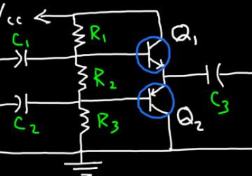
Figure 7 (a) is a commonly used low power drive circuit, which is simple, reliable and low cost. It is suitable for low power switchgear that does not require isolation. The drive circuit shown in figure 7 (b) has fast switching speed and strong drive capability. In order to prevent the two MOSFET tubes from going straight through, a 0.5 × 1 Ω low resistance is usually connected in series for current limiting. The circuit is suitable for medium power switchgear that does not require isolation. These two kinds of circuits are characterized by simple structure.
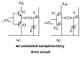
Fig 7.
Power MOSFET is a voltage type control device. As long as the voltage applied between the gate and the source exceeds its threshold voltage, it will be turned on. Because of the junction capacitance of MOSFET, the sudden rise of the voltage at both ends of the drain source will produce interference voltage at both ends of the gate source through the junction capacitance when it is turned off. The turn-off circuit of the commonly used complementary drive circuit has small impedance and fast turn-off speed, but it cannot provide negative pressure, so its anti-interference is poor. In order to improve the anti-interference of the circuit, a circuit composed of V1, V2 and R can be added to the drive circuit to produce a negative pressure. The circuit schematic diagram is shown in Fig. 8.
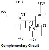
Fig 8.
When V1 is turned on, V 2 is turned off, the gate and source of the upper tube in the two MOSFET are discharged, and the gate and source of the lower tube are charged, that is, the upper tube is turned off and the lower tube is turned on, which is turned off by the driven power tube. On the contrary, when V1 is turned off, V 2 is turned on, the upper tube is turned on, and the lower tube is turned off thus to turn on the driven pipe. Because the gate and source of the upper and lower tubes are charged and discharged through different circuits, including the circuit of V 2 and because V2 will continue to exit saturation until it is turned off, it is slower for S1 to turn on than to turn off, and faster to turn on than to turn off for S2. Therefore, the degree of fever of the two tubes is not exactly the same; S1 is more serious than S2.
The disadvantage of the drive circuit is that it needs double power supply, and because the value of R cannot be too large, otherwise it will make V1 deeply saturated and affect the turn-off speed. So, there will be a certain loss on R.
4.1.2 Isolated drive circuit
Forward drive circuit
The circuit principle is shown in figure 9 (a). N3 is demagnetizing winding and S2 is the driven power tube. R2 is a damping resistance to prevent voltage oscillation at the gate and source end of the power tube. Because the leakage sense is not required to be small, and in terms of speed, R2 is generally small, so it is ignored in the analysis.
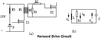
Fig 9.
Its equivalent circuit diagram, as shown in figure 9 (b), is a secondary side parallel resistor R1, which is not required for pulse and used as a false load of the forward converter to eliminate the misconduction caused by output voltage oscillations during the turn-off period. At the same time, it can also be used as an energy release circuit when the power MOSFET is turned off. The conduction speed of the drive circuit is mainly related to the driven S2 gate, the equivalent input capacitance of the source, the speed of the drive signal of S1 and the current provided by S1. From the simulation and analysis, we know that the smaller the duty ratio D, the larger R1, the larger L, the smaller the magnetization current, the smaller the U1 value, the slower the turn-off speed. The circuit has the following advantages:
The structure of the circuit is simple and reliable, and the isolated drive is realized;
Only a single power supply can provide positive pressure when on and negative pressure when off;
When the duty ratio is fixed, the drive circuit can have a fast switching speed through the reasonable parameter design.
The disadvantages of the circuit are as follows:
First, because the secondary side of the isolation transformer needs a false load to prevent oscillation, so the circuit loss is large; second, when the duty ratio changes, the turn-off speed changes greatly. When the pulse width is narrow, the turn-off speed of MOSFET gate becomes slower due to the decrease of stored energy.
A complementary drive circuit with an isolation transformer
As shown in figure 10, V1 and V2 are complementary, capacitance C acts as an isolated DC, and T1 is a magnetic ring or tank with high frequency and high magnetic flux.
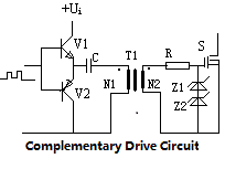
Fig 10.
The voltage on the isolation transformer is (1 / D) Ui when it is on and D Ui when it is turned off. If the voltage of the main power tube S by conduction is 12 V and the original side-to-turn ratio N1/N2 of the isolation transformer is 12 / [(1 / (1) Ui], the C value can be slightly larger in order to ensure the voltage stability of GS during the conduction period. The circuit has the following advantages:
The circuit structure is simple and reliable, and has the function of electrical isolation. The turn-off ability of the drive does not change when the pulse width changes;
The circuit only needs one power supply, that is, it works as a single power supply. The function of isolated capacitance C can provide a negative pressure when the driven tube is turned off, which accelerates the turn-off of the power tube and has high anti-interference ability;
However, one of the major disadvantages of the circuit is that the amplitude of the output voltage will change with the change of duty ratio. When D is small, the negative voltage is small, the anti-interference of the circuit becomes worse, and the positive voltage is higher, so we should pay attention to make its amplitude not exceed the allowable voltage of MOSFET gate. When D is greater than 0.5, the positive voltage of drive voltage is less than its negative voltage, so it should be noted that the negative voltage does not exceed the allowable voltage of MOAFET gate. Therefore, the circuit is more suitable for situations where the duty ratio is fixed or the duty ratio variation range is small or the duty ratio is less than 0.5.
Drive Circuit composed of Integrated Chip UC3724/3725
The circuit composition is shown in fig. 11. UC3724 is used to generate high frequency carrier signal, and the carrier frequency is determined by capacitance CT and resistance RT. In general, the carrier frequency is less than 600kHz, and high frequency modulation waves are generated at both ends of feet 4 and 6. After being isolated by high frequency small magnetic ring transformer, it is sent to feet 7 and 8 of UC3725 chip and modulated by UC3725 and the Drive signal is obtained. A Schottky rectifier bridge in UC3725 simultaneously rectifies the high frequency modulation waves of feet 7 and 8 into a DC voltage for drive power.Generally speaking, the higher the carrier frequency is, the shorter the drive delay time will be, but the anti-interference will become worse if it is too high. The larger the magnetization inductance of the isolation transformer is, the smaller the magnetization current, the less the UC3724 heat will be. However, with the increase of the number of turns, the influence of parasitic parameters becomes greater, and the anti-interference ability will also be weakened.According to the experimental data, it is concluded that for the signal whose switching frequency is less than 100kHz, it is better to choose (400 to 500) kHz carrier frequency, the transformer uses high magnetic conductivity such as 5K, 7K and other high frequency ring magnetic core, the original magnetization inductance is less than about 1 milligram. This kind of drive circuit is only suitable for the situation where the signal frequency is less than 100kHz. If the signal frequency relative carrier frequency is too high, the relative delay is too much, and the drive power is increased, and the heating temperature of UC3724 and UC3725 chips is higher. Therefore, the switching frequency above 100kHz can only be applied to the MOSFET with smaller pole capacitance. When switching frequency of 1kVA is less than 100kHz, it is a good drive circuit. The circuit has the following characteristics: single power supply, the control signal is isolated from the drive, and the structure is simple and small, especially suitable for the situation where the duty ratio is uncertain or the signal frequency is also changed.
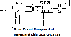
Fig 11.
 info@kynix.com
 00852-6915 1330


 0
0


