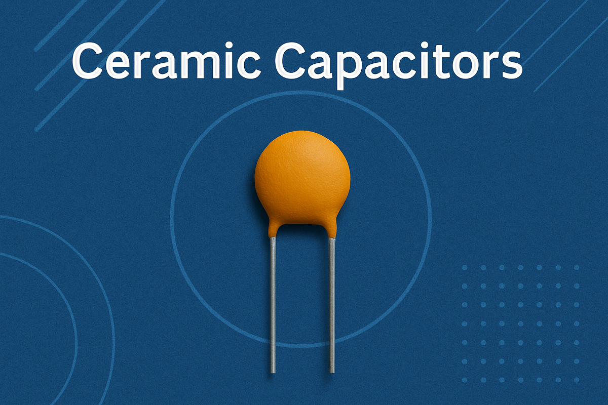
Catalog
| Introduction |
|
|
|
Design Flow of Chip |
Design | Specification Development |
| Design Details of the Chip |
| Draw a Blueprint for the Plane |
| About Wafer | What Is a Wafer |
|
| How to Make Single Crystal Wafer | Metallurgical Purification |
| Pulling the Crystal |
|
Design Flow of Chip |
Manufacture | What Is an IC Chip |
| Metal Sputtering |
| Coating Photoresistance |
| Etching Technology |
| Photoresist Removal |
|
Nano-Process
| What Is the Nano-Process |
| How Tiny Is the Nanometer |
| Purpose of Reducing the Process |
| Physical Limitations of Downsizing |
|
About Encapsulation
| Two Common Packages | DIP Package |
| BGA Package |
| Two Ways to Reduce Size
| SoC |
| SiP |
Introduction
A chip is a silicon chip that contains an integrated circuit, so the chip is also called an integrated circuit. It may be only 2.5 centimeters in square size, but it contains tens of millions of transistors. Simpler processors, on the other hand, may have thousands of transistors engraved on chips which are a few millimeters in size. Chip is the most important part of electronic equipment, which undertakes the function of operation and storage.
Design Flow of Chip
The birth of a chip can be divided into two parts: design and manufacture.
First, let's take a look at the complex and tedious chip design process.

Fig 1.
The process of making a chip is like building a house with Lego. First, the wafer is used as the foundation and the necessary IC chips can be produced after layers are stacked on top of each other. However, there is no use in having no amount of manufacturing capacity without a design drawing. Therefore, the role of an architect is very important.
But who is the architect in IC's design? The next step is to introduce the IC design.
In the IC production process, IC is mostly planned and designed by professional IC design companies, such as MediaTek, Qualcomm, Intel and other well-known large factories, all of which design their own IC chips to provide different specifications and efficiency chips for downstream manufacturers to choose from. Because IC is designed by the factories themselves, so IC design depends very much on the technology of engineers and the quality of engineers affects the value of an enterprise. But what are the steps engineers take to design an IC chip? The design process can be simply divided into the following steps.
Design
Specification Development
In IC design, the most important step is specification development. This step is like deciding how many rooms, bathrooms, what building codes to comply with, and designing after all the features have been identified so that no additional time is spent on subsequent modifications. The IC design needs to go through similar steps to ensure that the chip is designed without any errors.
The first step in specification development is to determine the purpose and effectiveness of IC and to set the general direction. The next step is to see what protocols to comply with, such as the wireless card chip needs to comply with IEEE 802.11 and other specifications. Otherwise, the chip will not be compatible with the products on the market, so that it will not be able to connect to other devices. Finally, the implementation method of this IC is established, different functions are allocated into different units, and the method of connecting different units is established, so that the specification can be completed.
Design Details of the Chip
After designing the specifications, it is followed by the details of the design chip. This step is like making a preliminary note of the planning of the building and depicting the overall outline for subsequent drawing. In IC chip, the hardware description language (HDL) is used to describe the circuit. The commonly used HDLs are Verilog, VHDL, and so on, which can easily express the function of a IC by code. This is followed by checking the correctness of the program's functionality and continuously modifying it until it meets the desired functionality.
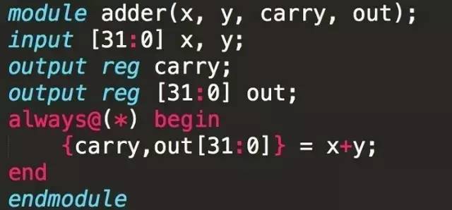
Fig 2. Verilog Example of 32 Bits Adder
Draw a Blueprint for the Plane
With a complete plan, the next step is to draw a blueprint for the plane. In IC design, the step of logic synthesis is to put the unmistakable HDL code into the electronic design automation tool (EDA tool), to let the computer convert HDL code into logic circuit, resulting in the following circuit diagram. After that, it is repeatedly determined whether the logic gate design conforms to the specification and is modified until the function is correct.
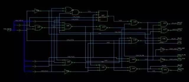
Fig 3. The Result of the Synthesis of the Control Unit
Finally, the synthesized code is put into another set of EDA tool for circuit layout and winding (Place And Route). After continuous detection, the following circuit diagram will be formed. You can see blue, red, green, yellow and other different colors, each of which represents a mask. As for the use of the mask, how should it be used?

Fig 4. The Commonly Used Calculus Chip-FFT Chip, Which Completes the Circuit Layout and the Winding Result
——The chip is stacked by layers of masks.
First of all, it is now known that an IC will produce multiple masks. These masks have the difference between the upper and lower layers and each layer has its own task. The following figure is a simple mask example. Taking the most basic element CMOS in the integrated circuit as an example, the full name of CMOS is complementary metal oxide semiconductor. That is, the combination of NMOS and PMOS to form CMOS. As for what is a metal oxide semiconductor (MOS)? This kind of component which is widely used in the chip is more difficult to explain, and it is more difficult for the general reader to figure it out, so there is no more detailed study here.
In the following figure, on the left is the circuit diagram formed after the circuit layout and winding, and you have already known that each color represents a mask. On the right is the way each mask is spread out. Production is to start from the bottom, in accordance with the method proposed in the manufacture of the IC chip, layer by layer, and finally the desired chip will be produced.
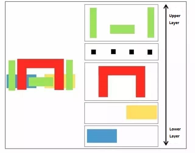
Fig 5.
At this point, you should have a preliminary understanding of the IC design. The overall view is very clear that IC design is a very complex major, but also thanks to the maturity of computer-aided software, so that IC design can be accelerated. The IC design relies heavily on the wisdom of engineers, and each of the steps described here has its own expertise and can be separated into multiple professional courses. For example, writing a hardware description language does not simply require familiarity with the programming language. You also need to understand how logic circuits work, how to convert the required algorithms into programs, and how synthetic software converts programs into logic gates.
What Is a Wafer?
In semiconductor news, it is always mentioned in the size of the wafer, such as 8-inch or 12-inch wafer. But what is the so-called wafer? What part of it is 8 inches? What is the difficulty of producing large wafers? Here is a step-by-step introduction to the most important foundation of semiconductors-what is a "wafer".
Wafer is the basis for making all kinds of computer chips. We can compare chip manufacturing to building a house with Lego blocks and building the shape we want (that is, all kinds of chips) by stacking one layer after another. However, if there is no good foundation, the built house will be tilted back and forth, contrary to our wishes. In order to make the perfect house, we need a smooth substrate. For chip manufacturing, this substrate is the wafer that will be described next.
First of all, think back to when you were a child playing with Lego blocks, there would be a small round bulge on the surface of the building blocks. With this structure, we can stack the two blocks firmly together without using glue. Chip manufacturing, also in a way like this, binds subsequent atoms to the substrate. Therefore, we need to find a substrate with a neat surface in order to meet the conditions needed for subsequent manufacturing.
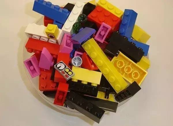
Fig 6.
In solid materials, there is a special crystal structure. That is, single crystal (Monocrystalline). It has the characteristics of atoms one after another closely arranged together, which can form a flat atomic surface. Therefore, using single crystal to make wafer can meet the above needs. However, how to produce such a material? There are two main steps, respectively, purification and crystal pulling. After this, such a material can be completed.
How to Make Single Crystal Wafer?
Metallurgical Purification
The purification is divided into two stages. The first step is metallurgical purification. During this process, we add carbon and convert silicon oxide into silicon with a purity of more than 98% in a redox manner. Most metals, such as iron or copper, are refined in this way to obtain sufficient purity of metal. However, 98% is still not enough for chip manufacturing and still needs to be further improved. Therefore, Siemens process will be used for purification, so that the high purity polysilicon needed for semiconductor process will be obtained.
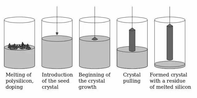
Fig 7. Silicon Column Manufacturing Process
Pulling the Crystal
Then there is the step of pulling the crystal. First, the high purity polysilicon obtained earlier is melted to form liquid silicon. After that, the single crystal silicon seed is in contact with the liquid surface and slowly pulls up as it rotates. As for why single crystal silicon is needed, that is because silicon atoms are arranged in the same way as people queue up. They will need to arrange the head so that later people can arrange it correctly. And silicon seed is an important row head, so that the later atoms know how to queue up. Finally, after the silicon atoms leaving the liquid surface solidify, the neatly arranged single crystal silicon columns are completed.
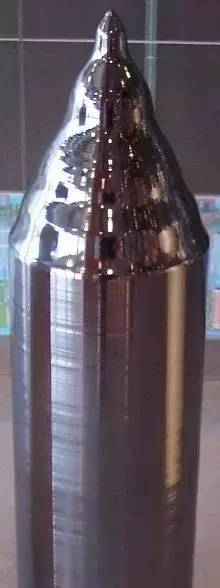
Fig 8. Single Crystal Silicon Column
But what do 8 inches and 12 inches stand for? It refers to the diameter of thin wafers being treated and sliced into,which is from the surface of the part of a crystal column that looks like a pencil rod. What is the difficulty of making large wafers? As mentioned earlier, the crystal column is made as if it were making marshmallows, rotating and forming at the same time. If you have made marshmallows, you should know that it is very difficult to make large and solid marshmallows, and the same is true of the crystal pulling process. The speed of rotation and the control of temperature will affect the quality of the crystal column. As a result, the larger the size, the higher the speed and temperature requirements are, so it is more difficult to make high-quality 12-inch wafers than 8-inch wafers.
However, a whole silicon column cannot be made into a chip-making substrate. In order to produce a silicon wafer, the silicon column needs to be cut transversely into a wafer with a diamond knife, and the wafer can be polished to form the silicon wafer needed for chip manufacturing. After so many steps, the fabrication of the chip substrate is complete, and the next step is to stack the house, that is, chip manufacturing. So, how to make a chip?
Manufacture
——Stacked chips
After introducing what silicon wafers are, you also know that making IC chips is like building a house with Lego blocks, creating the shape you want by stacking layer after layer. However, there are quite a few steps to build a house, and so is IC manufacturing. What are the steps to make IC? Next, the process of IC chip manufacturing will be introduced.
What Is an IC Chip?
Before we begin, we need to know what an IC chip is. IC, which means integrated circuit (Integrated Circuit), is the design of the circuit that is in the form of stacking together. In this way, we can reduce the area required to connect the circuit. The following figure is a 3D diagram of the IC circuit, from which you can see that its structure is like the beams and columns of a house. It is done layer by layer and this is the reason why IC manufacturing is compared to building a house.
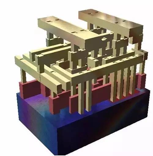
Fig 9. 3D Profile of IC Chip
From the 3D profile of the IC chip in the image above, the dark blue part at the bottom is the wafer introduced in the previous step. From this picture, we can see more clearly how important the wafer substrate plays in the chip. As for the red and khaki parts, they are the places to be completed when IC is made.
First of all, the red part can be compared to the hall on the first floor of the building. The hall on the first floor is the door of a house because everyone and everything come in and out of here. It has more functionality under the control of traffic. Therefore, compared with other floors, the construction will be more complex and requires more steps. In IC circuit, this hall is the logic gate layer; it is the most important part of the whole IC by combining a variety of logic gates together and completes the fully functional IC chip.
The yellow part is like a normal floor. Compared with the first floor, there will not be much complex structure, and each floor will not change much when it is built. The purpose of this layer is to connect the logic gates of the red part. The reason why so many layers are needed is that there are so many lines to be connected that a single layer cannot hold all the lines. So it is necessary to stack a few more layers to achieve this goal. Among them, the lines of different layers will be connected up and down to meet the needs of the wiring.
——Layered construction, layer by layer architecture
Once you know the construction of IC, let's show you how to make it. Imagine that if we want to make a fine drawing with a paint spray tank, we need to cut out the cover plate of the figure and cover it on paper. Then spray the paint evenly on the paper and remove the mask when the paint is dry. After repeating this step over and over again, you can complete neat and complex graphics. IC is made in a similar way, by covering up a layer of stacking.
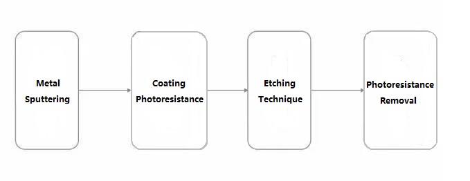
Fig 10.
When making IC, you can simply divide into the above four steps. Although the actual manufacturing steps will be different and the materials used will be different, but generally using a similar principle. This process is slightly different from painting: IC manufacturing is to paint first and then cover while painting is to cover and then paint. And the processes are described below.
Metal sputtering:
Sprinkle the metal material which is to be used evenly on the wafer to form a thin film.
Coating photoresistance:
First put the photoresist material on the wafer, and then hit the beam on the desired part through the mask to destroy the structure of the photoresist material. Next, use chemicals to wash away the damaged material.
Etching technology:
The silicon wafer without photoresistance protection will be etched by ion beam.
Photoresist removal:
Use the photoresist solution to dissolve the remaining photoresist, so that a process can be completed.
Finally, a lot of IC chips will be completed on a whole wafer, and then as long as the completed square IC chips are cut off, they can be sent to the packaging factory for packaging. What is the packaging factory? We'll have to explain it later.
Nano-Process
What is the nano-process?
Samsung and TSMC compete fiercely in advanced semiconductor processes because both of them want to take the lead in wafer contract manufacturing to win orders, which has almost become a battle between 14 nanometers and 16 nanometers. But what is the meaning of 14 nm and 16 nm, and where do they refer? What are the benefits and problems that will be brought about by the reduction of the process? Next we will give a brief description of the nano-process.
How tiny is the nanometer?
Before you start, you need to understand what nanometer really means. Mathematically, nanometers are 0.000000001 meters, but this is a pretty bad example. After all, we can only see a lot of zeros after the decimal point, but we don't actually feel it. If you compare it with the thickness of nail, it may be more obvious.
If you actually measure it with a ruler, you can tell that the thickness of the nail is about 0.0001 meters (0.1mm), that is to say, try to cut the side of a nail into 100000 lines, each of which is about one nanometer. From this, we can slightly imagine how tiny a nanometer is.
Purpose of Reducing the Process
After knowing how small the nanometer is, it is necessary to understand the purpose of reducing the process. The main purpose of reducing the transistor is to insert more transistors into smaller chips so that the chip will not become larger as a result of technological advances; second, it can increase the computational efficiency of the processor; moreover, reducing the volume can also reduce the power consumption. Finally, after the chip size is reduced, it is easier to plug into the mobile device to meet the needs of thinness and lightness in the future.
Come back to explore what the nano-process is and we will take 14 nm as an example. The process refers to the minimum size of 14 nm in the chip. The following figure shows the appearance of a traditional transistor, as an example. The main purpose of reducing transistor is to reduce power consumption, but which part needs to be reduced to achieve this goal? The L in the figure on the left is what we expect to shrink. By reducing the gate length, the current can be routed from the Drain side to the Source end in a shorter path (if you are interested, you can use Google to search for MOSFET, which will be explained in more detail).

Fig 11.
In addition, computers operate on 0 and 1. How can we use transistors to meet this purpose? The way to do this is to determine whether the transistor has current flow. When a voltage supply is made at the Gate (green square), the current will flow from the Drain to the Source, and if there is no supply voltage, the current will not flow, so that it can represent 1 and 0. (As to why 0 and 1 are used to judge, if you are interested, you can go to the Brin algebra. That is the way we use this method to make a computer.)
Physical Limitations of Downsizing
However, the process cannot be reduced indefinitely. When we narrow the transistor to about 20 nanometers, we will encounter problems in quantum physics, so that the transistor has a leakage phenomenon, offsetting the benefits of L. As a way to improve, the concept of FinFET (Tri-Gate) was imported, as shown in the figure above. The leakage caused by physical phenomena can be reduced by importing this technology.
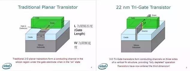
Fig 12.
More importantly, this method can increase the contact area between the Gate end and the lower layer. In traditional practice (top left), the contact surface has only one plane, but with FinFET (Tri-Gate), the contact surface will become three-dimensional, and the contact area can be easily increased. This allows the Source-Drain side to be smaller while maintaining the same contact area, which is of considerable help in reducing the size.
Finally, why would anyone say that it would be a pretty serious challenge for factories to enter the 10-nanometer process? It is mainly because the size of an atom is about 0.1 nanometers, and in the case of 10 nanometers, there are fewer than 100 atoms in a line. It is very difficult to make, and as long as there is an atomic defect, such as atoms falling out or impurities in the production process, there will be unknown phenomena, affecting the yield of the product.
If you can't imagine the difficulty, you can do a small experiment. Line up a 10 × 10 square with 100 small beads on the table, cut a piece of paper to cover the beads, then brush off the beads next to it with a small brush, and finally make it form a 10 × 5 rectangle. In this way, we can know the difficulties faced by the major factories and how difficult it is to achieve this goal.
Encapsulation
After a long process, from design to manufacture, finally we got an IC chip. However, a chip is so small and thin that it can be easily scratched and damaged if it is not protected from the outside. In addition, because of the small size of the chip, if you do not use a larger size of the shell, it will not be easy to manually place on the circuit board.
Therefore, the next step is to describe the encapsulation:
Two Common Packages
At present, there are two common packages; one is the DIP package, which is common in electric toys and looks like a centipede, the other is the BGA package, which is common when buying boxed CPU. As for other packaging methods, there are PGA (Pin Grid Array) used in the early CPU or an improved version of QFP (plastic square flat package) of DIP.
Because there are so many packaging methods, only DIP and BGA encapsulation are described below:
——Enduring Traditional Packaging
DIP Package
The first thing to introduce is the Dual Inline Package (DIP), we can see from the following figure that the IC chip with this package will look like a black centipede at the foot of the dual inline connection and this is the earliest IC packaging technology. It has the advantage of low cost and is suitable for small chips without too many wires. However, because most of them are plastic, the heat dissipation effect is poor, which cannot meet the requirements of the current high-speed chips. Therefore, most of the chips using this package are durable chips, such as OP741 shown in the following figure or smaller IC chips with less speed requirements and fewer holes.
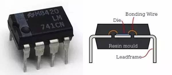
Fig 13.
The IC chip shown on the left is a common voltage amplifier named OP741.
On the right is its section. The package connects the chip to the leadframe with a gold wire.
BGA Package
As for spherical array (Ball Grid Array,BGA) packaging, compared with DIP, it is smaller and can be easily placed in smaller devices. In addition, because the pin is located under the chip, it can hold more metal pins than the DIP so it is Ideal for chips that require more contacts. However, the cost of this packaging method is high and the connection method is more complex, so it is mostly used in high unit price products.
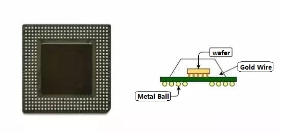
Fig 14.
On the left is a chip encapsulated in BGA. On the right is a schematic diagram of BGA using a cladding packaging.
——The rise of mobile devices and the emergence of new technologies on the stage
Two Ways to Reduce Size
However, the use of these packaging methods will cost a considerable amount of volume. For example, today's mobile devices, wearing devices, and so on, require quite a variety of components. If each component is packaged independently, it will cost a lot of space. Therefore, there are two ways to meet the requirements of reducing size. They are SoC (System On Chip) and SiP (System In Packet).
SoC
At the beginning of the rise of smart phones, the term SoC can be found in major financial magazines, but what is SoC? To put it simply, ICs with different functions are integrated into one chip. By this method, not only the volume can be reduced, but also the distance between different IC can be reduced, and the calculation speed of the chip can be improved. As for the manufacturing method, during the IC design phase, different ICs are put together and then a mask is made through the design process described earlier.
However, SoC is not the only advantage; to design a SoC requires considerable technical cooperation. When IC chips are encapsulated, they have their own external protection, and the distance between IC and IC is long, so there is no interactive interference. But when all the ICs are wrapped together, it is the beginning of a nightmare. The IC design factory has to change from the original simple design IC, to the IC which requires them to understand and integrate the various functions. Therefore, it increase the workload of engineers. In addition, there will also be a lot of situations, such as the high-frequency signal of the communication chip may affect the IC of other functions and so on.
In addition, SoC also needs to obtain IP (intellectual property) authorization from other vendors in order to put components designed by others into SoC. Because making SoC needs to obtain the design details of the whole IC in order to make a complete mask, which also increases the design cost of SoC. Some people may question why not just design one by yourself. That is because designing all kinds of IC requires a lot of knowledge related to the IC, only a rich enterprise like Apple can have a budget to poach top engineers from well-known enterprises. It's still a lot cheaper to design a whole new IC through collaborative licensing than to develop it by yourself.
SiP
As an alternative, SiP has leapt onto the stage of integrating chips. Unlike SoC, it buys IC from different enterprises and finishes the last step, which is to encapsulate the IC. In this way, the IP licensing step is eliminated and the design cost is significantly reduced. In addition, because they are independent ICs, the degree of interference with each other is greatly reduced.
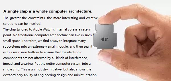
Fig 15.
Apple Watch uses SiP technology to package the entire computer architecture into a chip, not only to meet the desired performance but also to reduce the size, so that the watch has more space for battery release.
The most famous product using SiP technology is Apple Watch. Because the internal space of Watch is too small, it cannot use the traditional technology, the design cost of SoC is too high, SiP has become the first choice. With SiP technology, not only the volume can be reduced, but also the distance between each IC can be shortened, so SiP can be a feasible compromise. The following figure shows the structure of the Apple Watch chip, and you can see that quite a few IC are included in it.

Fig 16. Internal configuration Diagram of S1 Chip encapsulated by SiP in Apple Watch
After the packaging is completed, we will enter the testing stage. At this stage, it is necessary to confirm whether the encapsulated IC is functioning properly and that it can be shipped to the assembly plant after it is correct, so that the electronic products we can see can be made. So far, the semiconductor industry has completed the task of the whole production.
 info@kynix.com
 00852-6915 1330


 0
0


