The Kynix Components - Discrete Semiconductor Products
Stay Ahead with Expert Electronics Insights,
Industry Trends, and Innovative Tips
CatalogProduct Overview2N3055 Related Video Introduction2N3055 CAD Models2N3055 Internal Schematic Diagram2N3055 Features2N3055 Datasheet2N3055 Specifications2N3055 ManufacturerUsing Warning2N3055 FAQ Product OverviewThe 2N3055 is a silicon Epitaxial-Base Planar NPN transistor mounted in Jedec TO-3 metal case.It is intended for power switching circuits, series and shunt regulators, output stages and high fidelity amplifiers.The complementary PNP type is MJ2955. 2N3055 Related Video Introduction2N3055 Video Description: Hello guys, this is a class A amplifier circuit using transistors 2N3055 and C2073 paired Darlington, the circuit for quite a high amplification factor gives extremely powerful sound.This is the simplest circuit, easy to find components.Thank you for watching the video and for supporting me. Good luck. 2N3055 CAD ModelsFigure: 2N3055 PCB Symbol Figure: 2N3055 Footprint Figure: 2N3055 3D Models 2N3055 Internal Schematic DiagramFigure: 2N3055 Internal Schematic Diagram 2N3055 Features■ STMicroelectronics preferred salestypes■ Complementary NPN-PNP devices 2N3055 DatasheetYou can download the datasheet from the link given below:2N3055 Datasheet 2N3055 SpecificationsTypeDescriptionCategoryDiscrete Semiconductor ProductsTransistors - Bipolar (BJT) - SingleMfrSTMicroelectronicsPackageTrayPart StatusObsoleteTransistor TypeNPNCurrent - Collector (Ic) (Max)15 AVoltage - Collector Emitter Breakdown (Max)60 VVce Saturation (Max) @ Ib, Ic3V @ 3.3A, 10ACurrent - Collector Cutoff (Max)700µADC Current Gain (hFE) (Min) @ Ic, Vce20 @ 4A, 4VPower - Max115 WOperating Temperature200°C (TJ)Mounting TypeChassis MountPackage / CaseTO-204AA, TO-3Supplier Device PackageTO-3Base Product Number2N30 2N3055 ManufacturerSTMicroelectronics is a French-Italian multinational electronics and semiconductors manufacturer headquartered in Plan-les-Ouates near Geneva, Switzerland. The company resulted from the merger of two government-owned semiconductor companies in 1987: "Thomson Semiconducteurs" of France and "SGS Microelettronica" of Italy. It is commonly called "ST", and it is Europe's largest semiconductor chip maker based on revenue. While STMicroelectronics corporate headquarters and the headquarters for EMEA region are based in the Canton of Geneva, the holding company, STMicroelectronics N.V. is incorporated in the Netherlands. Using WarningNote: Please check their parameters and pin configuration before replacing them in your circuit. 2N3055 FAQWhat is 2N3055 transistor?The 2N3055 transistor is a diamond-shaped electronic device designed to control the movement of energy in larger operating systems. Transistors absorb volts and transform them into watts of energy. This transistor operates at 50 amperes (A), 60 volts (V), and 115 watts (W). Is 2N3055 a BJT?From the above posting we learned the main specifications and datasheet of the versatile workhorse transistor 2N3055. This transistor is a universal power BJT that can be used in almost all higher power based applications where high current and efficient switching of current is expected. What is 2N3055 used for?The 2N3055 transistor is used as a series pass transistor within linear power supplies and also used in high power and medium-current circuits like DC to AC inverters, low-frequency power converters, audio power amplifiers.
Kynix On 2021-11-26
Product OverviewSchottky diodes have very low forward drop voltage VF which makes them ideal for fast switching applications at lower current ratings. 1N5822 have forward voltage drop of minimum 0.525 V that is it requires 0.525 V to conduct in forward biased direction. The 1N5822 has maximum average forward rectified current IF(AV) of 3A. The maximum repetitive peak reverse voltage VRRM for 1N5822 is 40V. This blog will introduce 1N5822 systematically from its features, pinout to its specifications, applications, also including 1N5822 datasheet and so much more. CatalogProduct OverviewRelated Video Introduction1N5822 Features1N5822 Pinout1N5822 Pin Configuration1N5822 Applications1N5822 CAD Models1N5822 Circuit Diagram1N5822 Package1N5822 Specification1N5822 Manufacturer1N5822 DatasheetUsing Warnings1N5822 FAQ Related Video Introduction Video: Schottky Diode Explained 1N5822 Video Description: What is Schottky Diode: The Schottky diode is a two terminal device which works similar to the diode but has some unique features. 1) Low Forward Voltage Drop (Typically 0.3 V to 0.5V)2) Small Reverse Recovery Time Due to its Low Forward Voltage Drop, it is used in the high power applications. (High current and relatively low power applications) And due to its small reverse recovery time, it is used in the fast switching applications (e.g SMPS, communication devices (RF mixer and detector circuits) 1N5822 FeaturesExtremely Low VFLow Power Loss/High EfficiencyLow Stored Charge, Majority Carrier ConductionShipped in plastic bags, 500 per bagAvailable in Tape and Reel, 1500 per reel, by adding a “RL”suffix tothe part numberPb-Free Packages are Available 1N5822 PinoutThe following figure is the diagram of 1N5822 pinout. 1N5822 Pinout 1N5822 Pin ConfigurationPin NameDescriptionAnodeCurrent always Enters through AnodeCathodeCurrent always Exits through Cathode 1N5822 ApplicationsLow voltage high frequency invertersFreewheelingDc/dc convertersdetect signalsPolarity protection applicationsradio frequency (RF) applicationslogic circuits, due to fast switchingSchottky diodes are used in switched-mode power supplies 1N5822 CAD ModelsThe followings are 1N5822 Symbol, Footprint, and 3D Model. 1N5822 Symbol 1N5822 Footprint 1N5822 3D Model 1N5822 Circuit DiagramSchottky diode requires very low forward voltage to conduct in forward direction, therefore they are mostly used in power supply, fast switching applications etc. 1N5822 Circuit Diagram Above circuit shows the diode connected in forward biased inorder to switch ON/OFF the LED. The power source used in the circuit is 3.7V battery. As seen the Schottky diode operates at low voltage and the LED is switched ON. 1N5822 PackageThe following diagram shows the 1N5822 package. 1N5822 Package 1N5822 SpecificationProduct AttributeAttribute ValueManufacturer:ON SemiconductorProduct Category:Schottky Diodes & RectifiersMounting Style:Through HolePackage / Case:DO-201AD-2Configuration:SingleTechnology:SiIf - Forward Current:3 AVrrm - Repetitive Reverse Voltage:40 VVf - Forward Voltage:525 mVIfsm - Forward Surge Current:80 AIr - Reverse Current:2 mAMinimum Operating Temperature:- 65 CMaximum Operating Temperature:+ 150 CSeries:1N5822Height:5.3 mmLength:9.5 mmFactory Pack Quantity:600Width:5.3 mmUnit Weight:0.038801 oz 1N5822 ManufacturerON Semiconductor is a Fortune 500 company driving energy efficient innovations, empowering customers to reduce global energy use. The company is a leading supplier of semiconductor-based solutions, offering a comprehensive portfolio of energy efficient power and signal management, logic, standard and custom devices. The company’s products help engineers solve their unique design challenges in automotive, communications, computing, consumer, industrial, medical and military/aerospace applications. 1N5822 DatasheetYou can download 1N5822 datasheet from the link given below:1N5822 Datasheet Using WarningsNote: Please check their parameters and pin configuration before replacing them in your circuit. 1N5822 FAQWhat is a Schottky diode used for?Compared to p-n diodes, a Schottky diode provides lower voltage drop across the diode at low reverse bias. Some applications of Schottky diodes include rectifiers in switching regulators, discharge protection in power electronics, and rectifying circuits requiring high switching rate. What is the difference between diode and Schottky diode?Like other diodes, the Schottky diode controls the direction of current flow in a circuit. ... However, unlike standard diodes, the Schottky diode is known for its low forward voltage and fast switching ability. This makes them an ideal choice for radio frequency applications and any device with low voltage requirements. How do I choose a Schottky diode?For a Schottky diode this can be in the range 0.3 to 0.6 volts typically. The power ratings are based on not only how much current, but how much time the current will be flowing through the diode. If you have a continuous current then the power rating of the package needs to be more than what the diode is dissipating. What are the limitations of Schottky diodes?The most evident limitations of Schottky diodes are their relatively low reverse voltage ratings, and their relatively high reverse leakage current. For silicon-metal Schottky diodes, the reverse voltage is typically 50 V or less. What causes a Schottky diode to fail?Failure of schottky diodes during overstress conditions is usually a result of electrostatic discharge(ESD). Buildup of as little as 1000V – 1500V and the subsequent discharge are enough to damage these parts. Reverse bias is the most prevalent condition under which ESD takes place.
Kynix On 2021-11-25
Product OverviewThese N-Channel enhancement mode field effect transistors are produced using Fairchild's proprietary, high cell density, DMOS technology. These products have been designed to minimize on-state resistance while provide rugged, reliable, and fast switching performance. They can be used in most applications requiring up to 500mA DC.These products are particularly suited for low voltage, low current applications such as small servo motor control,power MOSFET gate drivers, and other switching applications. BS170 Related Video IntroductionBS170 Video Description: Each week I will grab a random electronic component from the vault and build a circuit - this week I look at how to hook up indicator LEDs to the PSU so we know when a voltage is "live". BS170 CAD ModelsFigure: BS170 PCB Symbol Figure: BS170 Footprint Figure: BS170 3D Models BS170 Switching Test CircuitFigure: BS170 Switching Test Circuit BS170 Features■ High density cell design for low RDS(ON).■ Voltage controlled small signal switch.■ Rugged and reliable.■ High saturation current capability BS170 DatasheetYou can download the datasheet from the link given below:BS170 Datasheet BS170 SpecificationsProduct AttributeAttribute ValueManufacturer:onsemiProduct Category:MOSFETTechnology:SiMounting Style:Through HolePackage / Case:TO-92-3Transistor Polarity:N-ChannelNumber of Channels:1 ChannelVds - Drain-Source Breakdown Voltage:60 VId - Continuous Drain Current:500 mARds On - Drain-Source Resistance:1.2 OhmsVgs - Gate-Source Voltage:- 20 V, + 20 VVgs th - Gate-Source Threshold Voltage:3 VOperating Temperature:-55~+150℃Pd - Power Dissipation:830 mWChannel Mode:EnhancementPackaging:BulkBrand:onsemi / FairchildConfiguration:SingleForward Transconductance - Min:0.32 SHeight:5.33 mmLength:5.2 mmProduct:MOSFET Small SignalProduct Type:MOSFETSeries:BS170Subcategory:MOSFETsTransistor Type:1 N-ChannelType:FETWidth:4.19 mmPart # Aliases:BS170_NLUnit Weight:0.016000 oz BS170 ManufacturerOnsemi is driving energy efficient innovations, empowering customers to reduce global energy use. The company offers a comprehensive portfolio of energy efficient power and signal management, logic, discrete and custom solutions to help design engineers solve their unique design challenges in automotive, communications, computing, consumer, industrial, LED lighting, medical, military/aerospace and power supply applications. onsemi operates a responsive, reliable, world-class supply chain and quality program, and a network of manufacturing facilities, sales offices and design centers in key markets throughout North America, Europe, and the Asia Pacific regions. Using WarningNote: Please check their parameters and pin configuration before replacing them in your circuit. BS170 FAQWhat is BS170?The BS170 is a N-channel enhancement mode Field Effect Transistor is produced using high cell density, DMOS technology. This very high density process has been designed to minimize on-state resistance while provide rugged, reliable and fast switching performance. How do MOSFETs work?It works by varying the width of a channel along which charge carriers flow (electrons or holes). The charge carriers enter the channel at source and exit via the drain. The width of the channel is controlled by the voltage on an electrode is called gate which is located between source and drain. Why do we use MOSFET?The MOSFET (Metal Oxide Semiconductor Field Effect Transistor) transistor is a semiconductor device which is widely used for switching and amplifying electronic signals in the electronic devices. The MOSFET works by varying the width of a channel along which charge carriers flow (holes and electrons).
Kynix On 2021-11-25
CatalogProduct Overview1N914 Related Video Introduction1N914 CAD Models1N914 Package Dimensions1N914 Features1N914 Applications1N914 Datasheet1N914 Specifications1N914 ManufacturerUsing Warning1N914 FAQ Product OverviewThis 1N914 JEDEC registered switching/signal diode features internal metallurgical bonded construction for military grade products per MIL-PRF-19500/116. This small low capacitance diode, with very fast switching speeds, is hermetically sealed and bonded into a double-plug DO-35 package. It may be used in a variety of very high speed applications including switchers, detectors, transient OR'ing, logic arrays, blocking, as well as low-capacitance steering diodes, etc. Microsemi also offers a variety of other switching/signal diodes. 1N914 Related Video IntroductionVideo Description: Provided to YouTube by Believe SAS1N914 · Yoo Doo Right · John Talbot · Charles Masson · Justin Cober · MothlandDon't Think You Can Escape Your Purpose 1N914 CAD ModelsFigure: 1N914 PCB Symbol Figure: 1N914 Footprint Figure: 1N914 3D Models 1N914 Package DimensionsFigure: 1N914 Package Dimensions 1N914 FeaturesJEDEC registered 1N914 number.Hermetically sealed glass construction.Metallurgically bonded.Double plug construction.Very low capacitance.Very fast switching speeds with minimal reverse recovery times.JAN, JANTX, and JANTXV qualifications are available per MIL-PRF-19500/116.RoHS compliant version available (commercial grade only). 1N914 ApplicationsHigh frequency data lines.Small size for high density mounting using flexiblethru-hole leads (see package illustration).RS-232 & RS–422 interface networks.Ethernet 10 base T.Low-capacitance steering diodes.LAN.Computers. 1N914 DatasheetYou can download the datasheet from the link given below:1N914 Datasheet 1N914 SpecificationsProduct AttributeAttribute ValueManufacturer:MicrochipProduct Category:Diodes - General Purpose, Power, SwitchingRoHS:NMounting Style:Through HolePackage / Case:DO-35-2Configuration:SingleVf - Forward Voltage:1.2 VIr - Reverse Current:5 uAMinimum Operating Temperature:- 65℃Maximum Operating Temperature:+ 175℃Packaging:BulkBrand:Microchip TechnologyLength:4.57 mmProduct Type:Diodes - General Purpose, Power, SwitchingSubcategory:Diodes & RectifiersUnit Weight:0.004833 oz 1N914 ManufacturerMicrochip Technology Inc. is a publicly-listed American corporation that manufactures microcontroller, mixed-signal, analog and Flash-IP integrated circuits. Its products include microcontrollers (PIC, dsPIC, AVR and SAM), Serial EEPROM devices, Serial SRAM devices, embedded security devices, radio frequency (RF) devices, thermal, power and battery management analog devices, as well as linear, interface and wireless products. Using WarningNote: Please check their parameters and pin configuration before replacing them in your circuit. 1N914 FAQWhat is a 1N914?1N914 is a small signal diode capable of handling low voltage and low current. The diode can be switched at high speed and therefore normally used in switching applications and not in rectifier applications. Is 1N914 the same as 1N4148?The 1N914 diode is considered equivalent to the 1N4148 diode. What type of diode is 1N914?The 1N914 is a small signal diode which can handle low voltage and low current. The diode can switch at high speed and hence normal used in switching applications and not in rectifier applications.
Kynix On 2021-11-25
CatalogProduct OverviewIRF540 Related Video IntroductionIRF540 CAD ModelsIRF540 Internal Schematic DiagramIRF540 Test CircuitsIRF540 FeaturesIRF540 ApplicationsIRF540 DatasheetIRF540 SpecificationsIRF540 ManufacturerUsing WarningIRF540 FAQ Product OverviewThis MOSFET series realized with STMicroelectronics unique STripFET process has specifically been designed to minimize input capacitance and gate charge. It is therefore suitable as primary switch in advanced highefficiency, high-frequency isolated DC-DC converters for Telecom and Computer applications. It is also intended for any applications with low gate drive requirements. IRF540 Related Video IntroductionIRF540 Video Description: Hello friends, In this video, you are going to know about IRF series MOSFET. IRF series MOSFET is more useful for switching heavy voltage applications using the small gate current. I have showed a small application for controlling a motor with a small base current using the proteus simulation software. IRF540 is an N-Channel MOSFET used for switching application. This MOSFET operates on enhancement mode. This mosfet is used in all kind of daily life applications like regulators, high speed power switching drivers, relay drivers and so on... This mosfet is also used for amplification processes. IRF540 CAD ModelsFigure: IRF540 PCB Symbol Figure: IRF540 Footprint Figure: IRF540 3D Models IRF540 Internal Schematic DiagramFigure: IRF540 Internal Schematic Diagram IRF540 Test CircuitsFigure: IRF540 Unclamped Inductive Load Test Circuit Figure: IRF540 Switching Times Test Circuits For Resistive Load Figure: IRF540 Gate Charge Test Circuit Figure: IRF540 Test Circuit For Inductive Load Switching And Diode Recovery Times IRF540 Features■ Typical RDS(on) = 0.055Ω■ Exceptional dv/dt capability■ 100% avalanche tested■ Low gate charge■ Application oriented characterization IRF540 Applications■ High-efficiency dc-dc converters■ UPS and motor control IRF540 DatasheetYou can download the datasheet from the link given below:IRF540 Datasheet IRF540 SpecificationsTypeDescriptionCategoryDiscrete Semiconductor ProductsTransistors - FETs, MOSFETs - SingleMfrSTMicroelectronicsSeriesSTripFET™ IIPackageTubePart StatusObsoleteFET TypeN-ChannelTechnologyMOSFET (Metal Oxide)Drain to Source Voltage (Vdss)100 VCurrent - Continuous Drain (Id) @ 25°C22A (Tc)Drive Voltage (Max Rds On, Min Rds On)10VRds On (Max) @ Id, Vgs77mOhm @ 11A, 10VVgs(th) (Max) @ Id4V @ 250µAGate Charge (Qg) (Max) @ Vgs41 nC @ 10 VVgs (Max)±20VInput Capacitance (Ciss) (Max) @ Vds870 pF @ 25 VPower Dissipation (Max)85W (Tc)Operating Temperature-55°C ~ 175°C (TJ)Mounting TypeThrough HoleSupplier Device PackageTO-220Package / CaseTO-220-3Base Product NumberIRF5 IRF540 ManufacturerSTMicroelectronics is a French-Italian multinational electronics and semiconductors manufacturer headquartered in Plan-les-Ouates near Geneva, Switzerland. The company resulted from the merger of two government-owned semiconductor companies in 1987: "Thomson Semiconducteurs" of France and "SGS Microelettronica" of Italy. It is commonly called "ST", and it is Europe's largest semiconductor chip maker based on revenue. While STMicroelectronics corporate headquarters and the headquarters for EMEA region are based in the Canton of Geneva, the holding company, STMicroelectronics N.V. is incorporated in the Netherlands. Using WarningNote: Please check their parameters and pin configuration before replacing them in your circuit. IRF540 FAQWhat is IRF540?IRF540 is an N-Channel powered MOSFET used for very fast switching operations as well as for amplification processes. It operates in enhancement mode. Its input impedance is quite high as compared to the general transistor so, its a lot sensitive in comparison to them. What are power MOSFETs used for?Power MOSFETs are widely used in transportation technology, which include a wide range of vehicles. In the automotive industry, power MOSFETs are widely used in automotive electronics. Power MOSFETs (including DMOS, LDMOS and VMOS) are commonly used for a wide range of other applications. What is N-channel Mosfet?A N-Channel MOSFET is a type of MOSFET in which the channel of the MOSFET is composed of a majority of electrons as current carriers. When the MOSFET is activated and is on, the majority of the current flowing are electrons moving through the channel.
Kynix On 2021-11-24
Product OverviewThe 2N4126 is a -25V PNP silicon Transistor capable of 625mW power dissipation and 800mA collector current. The NTE159 is designed for audio amplifier and switching applications. It is complementary to NTE123AP. This blog will introduce 2N4126 systematically from its features, pinout to its specifications, applications, also including 2N4126 datasheet and so much more. CatalogProduct OverviewRelated Video Introduction2N4126 Features2N4126 Pinout2N4126 Equivalents2N4126 DC Current Gain2N4126 Package2N4126 Specification2N4126 Manufacturer2N4126 DatasheetUsing Warnings2N4126 FAQ Related Video Introduction Video: Introduction to Bipolar Junction Transistor (BJT) 2N4126 Video Description: In this video, the Bipolar Junction Transistor, its different regions of operation, different configurations, and the working is briefly explained. 2N4126 Features-80V Collector to base voltage (VCBO)-5V Emitter to base voltage (VEBO)3°C/W Thermal resistance, junction to case200°C/W Thermal resistance, junction to ambient 2N4126 PinoutThe 2N4126 is manufactured in a plastic TO-92 case. When looking at the flat side with the leads pointed downward, the three leads emerging from the transistor are, from left to right, the emitter, base, and collector leads.Here is an image showing the pin diagram of the this transistor. 2N4126 Pinout 2N4126 EquivalentsYou can replace the 2N4126 with the 2SA642, 2SB564A, BCX79, KSA642, KSB564A, MPS4126, MPS6535, MPS6651, MPS6651G, MPS6652, MPS6652G, MPS750, MPS750G, MPSW51, MPSW51A, MPSW51AG, MPSW51G or PN200. 2N4126 DC Current GainThe following is the DC Current Gain of 2N4126. 2N4126 DC Current Gain 2N4126 PackageThe following diagram shows the 2N4126 package. 2N4126 Package 2N4126 SpecificationTYPEDESCRIPTIONCategoryTransistors - Bipolar (BJT) - SingleMfrNTE Electronics, IncPackageBagPart StatusActiveTransistor TypePNPCurrent - Collector (Ic) (Max)200 mAVoltage - Collector Emitter Breakdown (Max)25 VVce Saturation (Max) @ Ib, Ic400mV @ 5mA, 50mACurrent - Collector Cutoff (Max)50nA (ICBO)DC Current Gain (hFE) (Min) @ Ic, Vce120 @ 2mA, 1VPower - Max625 mWFrequency - Transition250MHzOperating Temperature-55C ~ 150C (TJ)Mounting TypeThrough HolePackage / CaseTO-226-3, TO-92-3 (TO-226AA)Supplier Device PackageTO-92 2N4126 ManufacturerFairchild is now part of onsemi together, we deliver a more extensive product portfolio of power discretes, ICs and power modules, plus a complete offering of low, mid and high voltage products across the entire voltage spectrum which means more choices for your designs. Together, we provide a stronger presence in the key markets of automotive, industrial and wireless, combined with increased technical and sales support. 2N4126 DatasheetYou can download 2N4126 datasheet from the link given below:2N4126 Datasheet Using WarningsNote: Please check their parameters and pin configuration before replacing them in your circuit. 2N4126 FAQWhat does a bipolar transistor do?A bipolar transistor allows a small current injected at one of its terminals to control a much larger current flowing between two other terminals, making the device capable of amplification or switching. What is the bipolar transistor device?A bipolar transistor is a semiconductor device commonly used for amplification. The device can amplify analog or digital signals. It can also switch DC or function as an oscillator. Physically, a bipolar transistor amplifies current, but it can be connected in circuits designed to amplify voltage or power. What is the difference between a FET and a bipolar transistor?The acronym of the BJT is Bipolar Junction Transistor and FET stands for Field Effect Transistor. The major difference between BJT and FET is that in a field-effect transistor only majority charge carries flows, whereas in BJT both majority and minority charge carriers flow. What is BJT and its types?BJTs are of two types namely NPN and PNP based on doping types of the three main terminals. An NPN transistor consists of two semiconductor junctions that have a thin p-doped anode region and PNP transistor also consists of two semiconductor junctions that have a thin n- doped cathode region. Why BJT is called bipolar?Bipolar transistors are a type of transistor composed of pn junctions, which are also called bipolar junction transistors (BJTs). Whereas a field-effect transistor is a unipolar device, a bipolar transistor is so named because its operation involves two kinds of charge carriers, holes and electrons.
Kynix On 2021-11-23
Join our mailing list!
Be the first to know about new products, special offers, and more.
Feature Posts
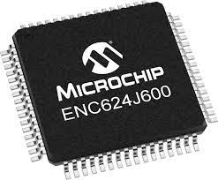
ENC624J600-I/PT microcontroller: Datasheet, Features, Application[FAQ]2023-03-07
ATMEGA1280-16AU microcontroller: Datasheet, Features, Application[FAQ]2023-03-07
STM8S207CBT6 Microcontroller: Datasheet, Features, Application[FAQ]2023-03-06
2N7002P Mosfet: Datasheet, Pinout, Features [FAQ]2021-10-21
L298N Motor Driver: Datasheet, Arduino, Circuit [Video&FAQ]2021-10-21