The Kynix Components - Discrete Semiconductor Products
Stay Ahead with Expert Electronics Insights,
Industry Trends, and Innovative Tips
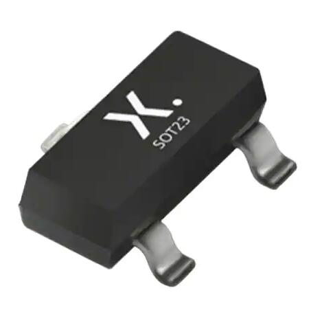
CatalogFeaturesMechanical DataBAV99 PinoutOrdering InformationMarking InformationMaximum RatingsThermal CharacteristicsElectrical CharacteristicsPackage Outline DimensionsIMPORTANT NOTICELIFE SUPPORTBAV99 DatasheetBAV99 FAQFeaturesFast Switching SpeedSurface Mount Package Ideally Suited for Automated InsertionFor General Purpose Switching ApplicationsTotally Lead-Free & Fully RoHS Compliant (Notes 1 & 2)Halogen and Antimony Free. “Green” Device (Notes 3 & 4)Qualified to AEC-Q101 Standards for High Reliability Mechanical DataCase: SOT23Case Material: Molded Plastic, “Green” Molding Compound UL Flammability Classification Rating 94V-0Moisture Sensitivity: Level 1 per J-STD-020Terminals: Matte Tin Finish Annealed over Alloy 42 Leadframe (Lead Free Plating). Solderable per MIL-STD-202, Method 208 e3Polarity: See DiagramWeight: 0.008 grams (Approximate)BAV99 PinoutThe following figure is the top view internal schematic of BAV99. BAV99 Top View Internal Schematic Ordering InformationPart NumberComplianceCasePackagingBAV99-7-FStandardSOT233,000/Tape & ReelBAV99-13-FStandardSOT2310,000/Tape & ReelBAV99Q-7-FAutomotiveSOT233,000/Tape & ReelBAV99Q-13-FAutomotiveSOT2310,000/Tape & Reel Notes:1.No purposely added lead . Fully EU Directive 2002/95/EC (RoHS), 2011/65/EU (RoHS 2) & 2015/863/EU (RoHS 3) compliant.2.See https://www.diodes.com/quality/lead-free/ for more information about Diodes Incorporated ’s definitions of Halogen - and Antimony-free, "Green" and Lead-free.3.Halogen- and Antimony-free "Green” products are defined as those which contain <900ppm bromine, <900ppm chlorine (<1500ppm total Br + Cl ) and <1000ppm antimony compounds.4.Product manufactured with Date Code 9W (week 39, 2009) and newer are built with Green Molding Compound. Product manufactured prior to Date Code 9W are built with Non-Green Molding Compound and may contain Halogens or Sb2O3 Fire Retardants. Marking Informationxx = JE, Product Type Marking Code YM = Date Code Marking for ShanghaiAssembly / Test site Y = Year (ex: F = 2018)M = Month (ex: 9 = September) Date Code KeyYear19981999…..201120122013201420152016201720182019202020212022CodeJK…..YZABCDEFGHIJ MonthJanFebMarAprMayJunJulAugSepOctNovDecCode123456789OND Maximum RatingsCharacteristicSymbolValueUnitNon-Repetitive Peak Reverse Voltage VRM 100VPeak Repetitive Reverse Voltage Working Peak Reverse Voltage DC Blocking VoltageVRRMVRWM VR 75 VRMS Reverse VoltageVR(RMS)53VForward Continuous Current (Note 6)IFM300mANon-Repetitive Peak Forward Surge Current @ t = 1.0µs@ t = 1.0sIFSM2.01.0A Thermal CharacteristicsCharacteristicSymbolValueUnitPower Dissipation (Note 6)PD350mWThermal Resistance Junction to Ambient Air (Note 6)RθJA357°C/WOperating and Storage Temperature RangeTJ, TSTG-65 to +150°C Electrical CharacteristicsCharacteristicSymbolMinMaxUnitTest ConditionReverse Breakdown Voltage (Note 7)V(BR)R75¾VIR = 2.5µA Forward Voltage VF ¾0.7150.8551.01.25 VIF = 1.0mA IF = 10mA IF = 50mAIF = 150mA Reverse Current (Note 7) IR ¾2.5503025µA µA µA nAVR = 75VVR = 75V, TJ = +150°C VR = 25V, TJ = +150°C VR = 20VTotal CapacitanceCT¾2.0pFVR = 0, f = 1.0MHzReverse Recovery Timetrr¾4.0nsIF = IR = 10mA,Irr = 0.1 x IR, RL = 100Ω Notes: 6. Part mounted on Polymide PC board with pad dimensions 1.13mm x 1.27mm.Short duration pulse test used to minimize self-heating effect. The following figures show the electrical characteristics of BAV99. Fig. 1 Power Derating Curve Fig. 2 Forward Characteristics Fig. 3 Typical Reverse Characteristics Fig. 4 Typical Capacitance vs. Reverse Voltage Package Outline DimensionsThe following diagram shows the BAV99 package. BAV99 Package IMPORTANT NOTICEDIODES INCORPORATED MAKES NO WARRANTY OF ANY KIND, EXPRESS OR IMPLIED, WITH REGARDS TO THIS DOCUMENT, INCLUDING, BUT NOT LIMITED TO, THE IMPLIED WARRANTIES OF MERCHANTABILITY AND FITNESS FOR A PARTICULAR PURPOSE (AND THEIR EQUIVALENTS UNDER THE LAWS OF ANY JURISDICTION). Diodes Incorporated and its subsidiaries reserve the right to make modifications, enhancements, improvements, corrections or other changes without further notice to this document and any product described herein. Diodes Incorporated does not assume any liability arising out of the application or use of this document or any product described herein; neither does Diodes Incorporated convey any license under its patent or trademark rights, nor the rights of others. Any Customer or user of this document or products described herein in such applications shall assume all risks of such use and will agree to hold Diodes Incorporated and all the companies whose products are represented on Diodes Incorporated website, harmless against all damages. Diodes Incorporated does not warrant or accept any liability whatsoever in respect of any products purchased through unauthorized sales channel. Should Customers purchase or use Diodes Incorporated products for any unintended or unauthorized application, Customers shall indemnify and hold Diodes Incorporated and its representatives harmless against all claims, damages, expenses, and attorney fees arising out of, directly or indirectly, any claim of personal injury or death associated with such unintended or unauthorized application. Products described herein may be covered by one or more United States, international or foreign patents pending. Product names and markings noted herein may also be covered by one or more United States, international or foreign trademarks. This document is written in English but may be translated into multiple languages for reference. Only the English version of this document is the final and determinative format released by Diodes Incorporated. LIFE SUPPORTDiodes Incorporated products are specifically not authorized for use as critical components in life support devices or systems without the express written approval of the Chief Executive Officer of Diodes Incorporated. As used herein: A.Life support devices or systems are devices or systems which: 1.are intended to implant into the body, or 2.support or sustain life and whose failure to perform when properly used in accordance with instructions for use provided in the labeling can be reasonably expected to result in significant injury to the user. B.A critical component is any component in a life support device or system whose failure to perform can be reasonably expected to cause the failure of the life support device or to affect its safety or effectiveness. Customers represent that they have all necessary expertise in the safety and regulatory ramifications of their life support devices or systems, and acknowledge and agree that they are solely responsible for all legal, regulatory and safety-related requirements concerning their products and any use of Diodes Incorporated products in such safety-critical, life support devices or systems, notwithstanding any devices- or systems-related information or support that may be provided by Diodes Incorporated. Further, Customers must fully indemnify Diodes Incorporated and its representatives against any damages arising out of the use of Diodes Incorporated products in such safety-critical, life support devices or systems. Copyright © 2018, Diodes Incorporated BAV99 DatasheetYou can download BAV99 datasheet from the link given below:BAV99 Datasheet BAV99 FAQWhy do we switch diodes?Diode is a two terminal PN junction that can be used in various applications. Hence the change of forward and reverse biased states makes the diode work as a switch, the forward being ON and the reverse being OFF state. What is a small signal diode used for?Small Signal Diodes are used in general purpose diode applications, high speed switching, parametric amplifiers and many other applications. Some important characteristics of Small Signal Diode are: Peak Reverse Voltage (VPR) – It is the maximum reverse voltage that can be applied to the diode before it breaks down. How do you test a small signal diode?You can use a multimeter or a simple tester (battery, resistor and LED) to check that a diode conducts in one direction but not the other. A lamp may be used to test a rectifier diode, but do NOT use a lamp to test a signal diode because the large current passed by the lamp will destroy the diode.
Kynix On 2021-12-15
Product OverviewThe TIP36C is a complementary PNP Power Transistor with low collector-emitter saturation voltage. It is manufactured in planar technology with base island layout. The resulting transistor show exceptional high gain performance coupled with very low saturation voltage. Designed for use in audio amplifier and general purpose applications. This blog will introduce TIP36C systematically from its features, pinout to its specifications, applications, also including TIP36C datasheet and so much more. CatalogProduct OverviewRelated Video IntroductionTIP36C FeaturesTIP36C PinoutTIP36C ApplicationsTIP36C CAD ModelsTIP36C Circuit DiagramInternal schematic diagramsTIP36C PackageTIP36C SpecificationTIP36C ManufacturerTIP36C DatasheetUsing WarningsTIP36C FAQ Related Video Introduction Video: tip35c tip36c amplificator audio 2x200w TIP36C Features■ Low collector-emitter saturation voltage■ Complementary NPN - PNP transistors TIP36C PinoutThe following figure is the diagram of TIP36C pinout. TIP36C Pinout TIP36C Applications■ General purpose■ Audio amplifier TIP36C CAD ModelsThe followings are TIP36C Symbol, Footprint, and 3D Model. TIP36C Symbol TIP36C Footprint TIP36C 3D Model TIP36C Circuit DiagramThe following is the circuit diagram of TIP36C. Test Circuit Inductive Load Switching Switching Time Equivalent Test Circuits Internal schematic diagramsThe following diagram shows the internal schematic diagrams. Internal schematic diagrams TIP36C PackageThe following diagram shows the TIP36C package. TIP36C Package TIP36C SpecificationProduct AttributeAttribute ValueManufacturer:STMicroelectronicsProduct Category:Bipolar Transistors - BJTMounting Style:Through HolePackage / Case:TO-247-3Transistor Polarity:PNPConfiguration:SingleCollector- Emitter Voltage VCEO Max:100 VCollector- Base Voltage VCBO:100 VEmitter- Base Voltage VEBO:- 5 VCollector-Emitter Saturation Voltage:1.8 VMaximum DC Collector Current:25 APd - Power Dissipation:125 WGain Bandwidth Product fT:3 MHzMinimum Operating Temperature:- 65 CMaximum Operating Temperature:+ 150 CSeries:TIP36CContinuous Collector Current:25 AHeight:20.15 mmLength:15.75 mmSubcategory:TransistorsTechnology:SiWidth:5.15 mmUnit Weight:0.229281 oz TIP36C ManufacturerSTMicroelectronics is a global independent semiconductor company and a leader in developing and delivering semiconductor solutions across the spectrum of microelectronics applications. An unrivaled combination of silicon and system expertise, manufacturing strength, Intellectual Property (IP) portfolio, and strategic partners positions, STMicroelectronics is at the forefront of System-on-Chip (SoC) technology and its products play a key role in enabling today's convergence trends. TIP36C DatasheetYou can download TIP36C datasheet from the link given below:TIP36C Datasheet Using WarningsNote: Please check their parameters and pin configuration before replacing them in your circuit. TIP36C FAQWhat does a bipolar transistor do?A bipolar transistor is a semiconductor device commonly used for amplification. The device can amplify analog or digital signals. It can also switch DC or function as an oscillator. Physically, a bipolar transistor amplifies current, but it can be connected in circuits designed to amplify voltage or power. What is called bipolar transistor?Bipolar transistors are a type of transistor composed of pn junctions, which are also called bipolar junction transistors (BJTs). Whereas a field-effect transistor is a unipolar device, a bipolar transistor is so named because its operation involves two kinds of charge carriers, holes and electrons. What is the function of BJT?The main basic function of a BJT is to amplify current it will allow BJTs are used as amplifiers or switches to produce wide applicability in electronic equipment include mobile phones, industrial control, television, and radio transmitters. There are two different types of BJTs are available, they are NPN and PNP.
Kynix On 2021-12-14
CatalogProduct OverviewMBR0520LT1G Related Video IntroductionMBR0520LT1G CAD ModelsMBR0520LT1G Marking DiagramMBR0520LT1G FeaturesMBR0520LT1G Mechanical CharacteristicsMBR0520LT1G DatasheetMBR0520LT1G SpecificationsMBR0520LT1G ManufacturerUsing WarningMBR0520LT1G FAQ Product OverviewThe Schottky Power Rectifier employs the Schottky Barrier principle with a barrier metal that produces optimal forward voltage drop−reverse current tradeoff. Ideally suited for low voltage, high frequency rectification, or as free wheeling and polarity protection diodes in surface mount applications where compact size and weight are critical to the system. This package provides an alternative to the leadless 34 MELF style package. MBR0520LT1G Related Video IntroductionMBR0520LT1G Video Description: Difference Between Diode, Schottky and Zener Diode: 1. Rectifier Diode: Rectifier diode is the simplest p-n junction diode , used mostly for rectification purposes in a half bridge and full bridge rectifier. 2. Schottky Diode Unlike a rectifier diode, junction of schottky diode is between n-type semiconductor to a metal plate. Schottky diode also known as barrier diode is mainly used in low voltage circuits because fwd voltage drop of schottky diode(Vf) is less then a rectifier diode typically in the range of .25 to .5 v. 3. Zener Diode: Zener diode is made up of p-n junction but heavily doped compared to a normal diode. As a result, it can undergo break down without being damaged. And Due to this property only, zener is used as a voltage regulator in electronic circuits. In fact, zener diodes are never used for rectification purposes.MBR0520LT1G CAD ModelsFigure: MBR0520LT1G PCB Symbol Figure: MBR0520LT1G Footprint Figure: MBR0520LT1G 3D Models MBR0520LT1G Marking DiagramFigure: MBR0520LT1G Marking DiagramB2 = Device CodeM = Date CodeMicrodot = Pb−Free Package(Note: Microdot may be in either location) MBR0520LT1G FeaturesGuardring for Stress ProtectionVery Low Forward Voltage (0.38 V Max @ 0.5 A, 25℃)125℃Operating Junction TemperatureEpoxy Meets UL 94 V−0 @ 0.125 inPackage Designed for Optimal Automated Board AssemblyAEC−Q101 Qualified and PPAP CapableSBR8 Prefix for Automotive and Other Applications RequiringUnique Site and Control Change RequirementsAll Packages are Pb−Free* MBR0520LT1G Mechanical CharacteristicsPolarity Designator: Cathode BandWeight: 11.7 mg (approximately)Case: Epoxy, MoldedFinish: All External Surfaces Corrosion Resistant andTerminal Leads are Readily SolderableLead and Mounting Surface Temperature for Soldering Purposes:260℃ Max. for 10 SecondsESD Ratings: Human Body Model = 3B Machine Model = C MBR0520LT1G DatasheetYou can download the datasheet from the link given below:MBR0520LT1G Datasheet MBR0520LT1G SpecificationsProduct AttributeAttribute ValueManufacturer:onsemiProduct Category:Schottky Diodes & RectifiersProduct:Schottky DiodesMounting Style:SMD/SMTPackage / Case:SOD-123-2Configuration:SingleTechnology:SiIf - Forward Current:500 mAVrrm - Repetitive Reverse Voltage:20 VVf - Forward Voltage:385 mVIfsm - Forward Surge Current:5.5 AIr - Reverse Current:250 uAOperating Temperature:-65°C ~ 125°CSeries:MBR0520LBrand:onsemiHeight:1.12 mmLength:2.69 mmProduct Type:Schottky Diodes & RectifiersSubcategory:Diodes & RectifiersTermination Style:SMD/SMTType:Schottky DiodeWidth:1.6 mmPart # Aliases:MBR0520LT3GUnit Weight:0.001058 oz MBR0520LT1G ManufacturerOnsemi is driving energy efficient innovations, empowering customers to reduce global energy use. The company offers a comprehensive portfolio of energy efficient power and signal management, logic, discrete and custom solutions to help design engineers solve their unique design challenges in automotive, communications, computing, consumer, industrial, LED lighting, medical, military/aerospace and power supply applications. onsemi operates a responsive, reliable, world-class supply chain and quality program, and a network of manufacturing facilities, sales offices and design centers in key markets throughout North America, Europe, and the Asia Pacific regions. Using WarningNote: Please check their parameters and pin configuration before replacing them in your circuit. MBR0520LT1G FAQWhat is MBR0520LT1G?The MBR0520LT1G from On Semiconductor is surface mount, single schottky power rectifier in SOD-123 package. This device is intended for use in low voltage, high frequency rectification, freewheeling and polarity protection applications. What is power Schottky rectifier?Schottky rectifiers have been used for over 25 years in the power supply industry. The primary advantages are very low forward voltage drop and switching speeds that approach zero time making them ideal for output stages of switching power supplies. How does a Schottky rectifier work?In a Schottky diode, a semiconductor–metal junction is formed between a semiconductor and a metal, thus creating a Schottky barrier. The N-type semiconductor acts as the cathode and the metal side acts as the anode of the diode. This Schottky barrier results in both a low forward voltage drop and very fast switching. What is the purpose of a Schottky diode?Schottky diodes are used for their low turn-on voltage, fast recovery time and low-loss energy at higher frequencies. These characteristics make Schottky diodes capable of rectifying a current by facilitating a quick transition from conducting to blocking state. What metal is used in Schottky diode?A metal-semiconductor junction is formed between a metal and a semiconductor, creating a Schottky barrier instead of a semiconductor-semiconductor junction as in conventional diodes. The semiconductor would typically be N-type silicon and typical metals used are molybdenum, platinum, chromium or tungsten.
Kynix On 2021-12-14
CatalogProduct OverviewP2N2222A Related Video IntroductionP2N2222A CAD ModelsP2N2222A Marking DiagramP2N2222A Switching Time Equivalent Test CircuitsP2N2222A FeaturesP2N2222A DatasheetP2N2222A SpecificationsP2N2222A ManufacturerUsing WarningP2N2222A FAQ Product OverviewThe NPN Bipolar Transistor is designed for use in linear and switching applications. The device is housed in the TO-92 package, which is designed for medium power applications. P2N2222A Related Video IntroductionP2N2222A Video Description: In this video I am going to explain to you how a BJT functions. What does it contains?Three terminals and an electron/hole charge carrier What can it do?Act as a switch and amplify current P2N2222A CAD ModelsFigure: P2N2222A PCB Symbol Figure: P2N2222A Footprint P2N2222A Marking DiagramFigure: P2N2222A Marking DiagramP2N2 = Device Code222A = Specific DeviceA = Assembly LocationY = YearWW = Work WeekMicrodot = Pb−Free Package(Note: Microdot may be in either location) P2N2222A Switching Time Equivalent Test CircuitsFigure: P2N2222A Turn−On Time Figure: P2N2222A Turn−Off Time P2N2222A FeaturesSmall Compact Surface Mountable Package with J-Bend LeadsRectangular Package for Automated HandlingHighly Stable Oxide Passivated JunctionLow Forward Voltage Drop (0.71 to 1.05 Volts Max @ 3.0 A, TJ = 150 C) Mechanical Characteristics:Case: Epoxy, MoldedWeight: 217 mg (approximately)Finish: All External Surfaces Corrosion Resistant and TerminalLeads are Readily SolderableLead and Mounting Surface Temperature for Soldering Purposes: 260 C Max. for 10 SecondsShipped in 16 mm Tape and Reel, 2500 units per reelPolarity: Notch in Plastic Body Indicates Cathode LeadThese are Pb-Free Devices P2N2222A DatasheetYou can download the datasheet from the link given below:P2N2222A Datasheet P2N2222A SpecificationsTypeDescriptionCategoryDiscrete Semiconductor ProductsTransistors - Bipolar (BJT) - SingleMfronsemiPackageBulkPart StatusObsoleteTransistor TypeNPNCurrent - Collector (Ic) (Max)600 mAVoltage - Collector Emitter Breakdown (Max)40 VVce Saturation (Max) @ Ib, Ic1V @ 50mA, 500mACurrent - Collector Cutoff (Max)10nADC Current Gain (hFE) (Min) @ Ic, Vce100 @ 150mA, 10VPower - Max625 mWFrequency - Transition300MHzOperating Temperature-55°C ~ 150°C (TJ)Mounting TypeThrough HolePackage / CaseTO-226-3, TO-92-3 Long BodySupplier Device PackageTO-92 (TO-226)Base Product NumberP2N222 P2N2222A ManufacturerOnsemi is driving energy efficient innovations, empowering customers to reduce global energy use. The company offers a comprehensive portfolio of energy efficient power and signal management, logic, discrete and custom solutions to help design engineers solve their unique design challenges in automotive, communications, computing, consumer, industrial, LED lighting, medical, military/aerospace and power supply applications. onsemi operates a responsive, reliable, world-class supply chain and quality program, and a network of manufacturing facilities, sales offices and design centers in key markets throughout North America, Europe, and the Asia Pacific regions. Using WarningNote: Please check their parameters and pin configuration before replacing them in your circuit. P2N2222A FAQWhat are amplifier transistors?A transistor acts as an amplifier by raising the strength of a weak signal. The DC bias voltage applied to the emitter base junction, makes it remain in forward biased condition. Thus a small input voltage results in a large output voltage, which shows that the transistor works as an amplifier. What are transistor amplifiers used for?Amplifiers are derived from the transistors because they are capable of operating under three regions active, cut-off and saturation. For the purpose of amplification, the focus will be on the active region. The main purpose of these amplifiers is to enhance the strength of the applied input signal without alteration. What are the types of transistor amplifier?Three of the most fundamental transistor amplifiers are: common emitter, common collector and common base. In each of the three configurations one of the three nodes is permanently tied to a common voltage (usually ground), and the other two nodes are either an input or output of the amplifier.
Kynix On 2021-12-13
Product OverviewThe IR MOSFET family of power MOSFETs utilizes proven silicon processes offering designers a wide portfolio of devices to support various applications such as DC motors, inverters, SMPS, lighting, load switches as well as battery powered applications.The devices are available in a variety of surface mount and through-hole packages with industry standard footprints for ease of design. This blog will introduce IRFP064N systematically from its features, pinout to its specifications, applications, also including IRFP064N datasheet and so much more. CatalogProduct OverviewIRFP064N FeaturesIRFP064N PinoutIRFP064N EquivalentsIRFP064N CAD ModelsIRFP064N Circuit DiagramIRFP064N PackageIRFP064N SpecificationIRFP064N ManufacturerIRFP064N DatasheetUsing WarningsIRFP064N FAQ IRFP064N FeaturesAdvanced Process TechnologyUltra Low On-ResistanceDynamic dv/dt Rating175°C Operating TemperatureFast SwitchingFully Avalanche Rated IRFP064N PinoutThe following figure is the diagram of IRFP064N pinout.VDSS = 55VRDS(on) = 0.008ΩID = 110A† IRFP064N Pinout IRFP064N EquivalentsYou can replace the IRFP064N with the IRFP1405, IRFP2907, IRFP2907Z, IRFP3077, IRFP3206, IRFP3306, IRFP4110, IRFP4310Z, IRFP4368, IRFP4468, IRFP4568. IRFP064N CAD ModelsThe followings are IRFP064N Symbol, Footprint, and 3D Model. IRFP064N Symbol IRFP064N Footprint IRFP064N 3D Model IRFP064N Circuit DiagramThe following is the circuit diagram of IRFP064N. Switching Time Test Circuit IRFP064N PackageThe following diagram shows the IRFP064N package. IRFP064N Package IRFP064N SpecificationProduct AttributeAttribute ValueManufacturer:InfineonProduct Category:MOSFETTechnology:SiMounting Style:Through HolePackage / Case:TO-247-3Transistor Polarity:N-ChannelNumber of Channels:1 ChannelVds - Drain-Source Breakdown Voltage:55 VId - Continuous Drain Current:110 ARds On - Drain-Source Resistance:8 mOhmsVgs - Gate-Source Voltage:- 20 V, + 20 VMinimum Operating Temperature:- 55 CMaximum Operating Temperature:+ 175 CPd - Power Dissipation:200 WChannel Mode:EnhancementBrand:Infineon / IRConfiguration:SingleFall Time:70 nsHeight:20.7 mmLength:15.87 mmProduct Type:MOSFETRise Time:100 nsSubcategory:MOSFETsTransistor Type:1 N-ChannelTypical Turn-Off Delay Time:43 nsTypical Turn-On Delay Time:14 nsWidth:5.31 mmUnit Weight:0.211644 oz IRFP064N ManufacturerInfineon Technologies is a leading global designer, manufacturer and supplier of a broad range of semiconductors used in various microelectronic applications. Infineon's product portfolio consists of logic products, including digital, mixed-signal, and analog integrated circuits, as well as discrete semiconductor products. IRFP064N DatasheetYou can download IRFP064N datasheet from the link given below:IRFP064N Datasheet Using WarningsNote: Please check their parameters and pin configuration before replacing them in your circuit. IRFP064N FAQWhat is MOSFET and how it works?MOSFET (metal-oxide semiconductor field-effect transistor, pronounced MAWS-feht ) is a special type of field-effect transistor ( FET ) that works by electronically varying the width of a channel along which charge carriers ( electron s or hole s) flow. The wider the channel, the better the device conducts. What is a MOSFET used for?MOSFET, in short, is a metal oxide semiconductor field-effect transistor used to switch or amplify voltages in circuits. What is the difference between Transistor and Mosfet?The only difference is in function. A MOSFET is a type of transistor commonly used in switching/amplifier type applications, as they are usually designed for higher power use (so called “high power” transistors are mostly MOSFET and Darlington type). Which is the another name of MOSFET?The metal–oxide–semiconductor field-effect transistor (MOSFET, MOS-FET, or MOS FET), also known as the metal–oxide–silicon transistor (MOS transistor, or MOS), is a type of insulated-gate field-effect transistor that is fabricated by the controlled oxidation of a semiconductor, typically silicon. Who invented the MOSFET?Martin (John) M. Atalla. John Atalla is one of the inventors of the metal-oxide-semiconductor field-effect transistor (MOSFET), the most widely employed type of integrated circuit. Born in Port Said, Egypt, Atalla came to the United States for graduate studies at Purdue University.
Kynix On 2021-12-09
CatalogULN2803A DescriptionULN2803A Related Video InstructionULN2803A CAD ModelsULN2803A PriceULN2803A Pin ConfigurationULN2803A FeaturesULN2803A Schematic DiagramsULN2803A DatasheetULN2803A SpecificationsULN2803A ManufacturerUsing WarningULN2803A FAQULN2803A DescriptionThe ULN2801A, ULN2802A, ULN2803A and ULN2804A each contain eight Darlington transistors with common emitters and integral suppression diodes for inductive loads. Each Darlington features a peak load current rating of 600 mA (500 mA continuous) and can withstand at least 50 V in the OFF state. Outputs may be paralleled for higher current capability. Four versions are available to simplify interfacing to standard logic families: the ULN2801A is designed for general purpose applications with a current limit resistor; the ULN2802A has a 10.5 kW input resistor and Zener for 14-25 V PMOS; the ULN2803A has a 2.7 kW input resistor for 5 V TTL and CMOS; the ULN2804A has a 10.5 kW input resistor for 6-15 V CMOS. All types are supplied in an 18-lead plastic DIP with a copper lead form and feature the convenient input-opposite-output pinout to simplify board layout. ULN2803A Related Video InstructionVideo: ULN2803A darlington transistor array driver ICULN2803A Video Description: Give the output logic of your microcontroller projects more current and voltage to drive larger loads with this simple to use chip. ULN2803A CAD Models Figure: PCB Symbol Figure: Footprint Figure: 3D Model ULN2803A PriceSuppliersFromIn stockDelivery(Day)MOQCurrency1+10+100+1K+10K+Arrow USA2323Immediate1USD $1.2841.1011.0071.0071.007Digi-KeyUSA21129Immediate1USD $1.61.4261.1120.7980.798VericalUSA0Immediate0USD $-0.4340.4340.4340.434AMEYA360HongKong20-1USD $0.4220.4220.4220.4220.422JLCShop-0Immediate1USD $0.6380.4740.4130.3930.393TME-330Immediate1USD $0.850.5160.4430.3840.384 ULN2803A Pin Configuration Figure: Pin Configuration ULN2803A FeaturesEight Darlington transistors with common emittersOutput current to 500 mAOutput voltage to 50 VIntegral suppression diodesVersions for all popular logic familiesOutput can be paralleledInputs pinned opposite outputs to simplify board layout ULN2803A Schematic Diagrams Figure: Schematic Diagrams ULN2803A DatasheetYou can download the datasheet from the link given below:ULN2803A-Datasheet ULN2803A SpecificationsManufacturer:STMicroelectronicsProduct Category:Darlington TransistorsConfiguration:OctalTransistor Polarity:NPNCollector- Emitter Voltage VCEO Max:50 VMaximum DC Collector Current:0.5 AMounting Style:Through HolePackage / Case:PDIP-18Minimum Operating Temperature:- 20 ℃Maximum Operating Temperature:+ 85 ℃Series:ULN2803APackaging:TubeBrand:STMicroelectronicsContinuous Collector Current:500 mAHeight:3.68 mmLength:23.24 mmProduct Type:Darlington TransistorsFactory Pack Quantity:1000Subcategory:TransistorsWidth:7.1 mmUnit Weight:0.045856 oz ULN2803A ManufacturerSTMicroelectronics is a French-Italian multinational electronics and semiconductors manufacturer headquartered in Plan-les-Ouates near Geneva, Switzerland. The company resulted from the merger of two government-owned semiconductor companies in 1987: "Thomson Semiconducteurs" of France and "SGS Microelettronica" of Italy. It is commonly called "ST", and it is Europe's largest semiconductor chip maker based on revenue. While STMicroelectronics corporate headquarters and the headquarters for EMEA region are based in the Canton of Geneva, the holding company, STMicroelectronics N.V. is incorporated in the Netherlands. Using WarningNote: Please check their parameters and pin configuration before replacing them in your circuit. ULN2803A FAQWhat are Darlington transistors used for?Darlington transistors are mainly used in switching and amplification applications for delivering a very high DC current gain. Some of the key applications are high and low side switches, sensor amplifiers and audio amplifiers. Is a Darlington transistor a Mosfet?MOSFETS can handle more current safely at lower temps and with fewer areas of weakness. I understand that MOSFETs are essentially a pair of darlington transistors with resistors and diodes built into a package. What is another name for a Darlington transistor?A Darlington Transistor configuration, also known as a “Darlington pair” or “super-alpha circuit”, consist of two NPN or PNP transistors connected together so that the emitter current of the first transistor TR1 becomes the base current of the second transistor TR2.
Kynix On 2021-12-09
Join our mailing list!
Be the first to know about new products, special offers, and more.
Feature Posts
ENC624J600-I/PT microcontroller: Datasheet, Features, Application[FAQ]2023-03-07
ATMEGA1280-16AU microcontroller: Datasheet, Features, Application[FAQ]2023-03-07
STM8S207CBT6 Microcontroller: Datasheet, Features, Application[FAQ]2023-03-06
2N7002P Mosfet: Datasheet, Pinout, Features [FAQ]2021-10-21
L298N Motor Driver: Datasheet, Arduino, Circuit [Video&FAQ]2021-10-21