Phone

    00852-6915 1330

The Kynix Components - Discrete Semiconductor Products

Stay Ahead with Expert Electronics Insights,
Industry Trends, and Innovative Tips

Discrete Semiconductor Products

BS250 P-Channel 60-V (D-S) MOSFET

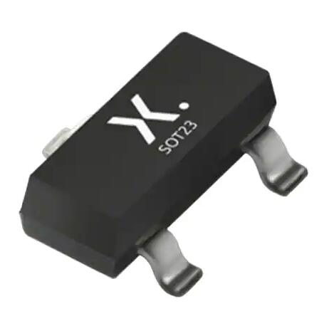
CatalogProduct SummaryBS250 FeaturesBS250 BenefitsBS250 ApplicationsBS250 PinoutAbsolute Maximum RatingsBS250 SpecificationsTypical CharacteristicsDisclaimerBS250 DatasheetUsing Warnings Product SummaryPart NumberV(BR)DSS Min (V)rDS(on) Max (Ω)VGS(th) (V)ID (A)TP0610L−6010 @ VGS = −10 V−1 to −2.4−0.18TP0610T−6010 @ VGS = −10 V−1 to −2.4−0.12VP0610L−6010 @ VGS = −10 V−1 to −3.5−0.18VP0610T−6010 @ VGS = −10 V−1 to −3.5−0.12BS250−4514 @ VGS = −10 V−1 to −3.5−0.18 BS250 FeaturesHigh-Side SwitchingLow On-Resistance: 8 QLow Threshold: -1.9 VFast Switching Speed: 16 nsLow Input Capacitance: 15 pF BS250 BenefitsEase in Driving Switches Low Offset (Error) VoltageLow-Voltage OperationHigh-Speed SwitchingEasily Driven Without Buffer BS250 ApplicationsDrivers: Relays, Solenoids, Lamps,Hammers, Displays, Memories,Transistors, etc.Battery Operated SystemsPower Supply, Converter CircuitsMotor Control BS250 PinoutThe following figures are the diagrams of BS250 pinout. TO-226AA (TO-92) TO-92-18RM TO-236 (SOT-23) Absolute Maximum RatingsParameterSymbolTP0610LTP0610TVP0610LVP0610TBS250UnitDrain-Source VoltageVDS−60−60−60−60−45 VGate-Source VoltageVGSt30t30t30t30t25 Continuous Drain Current (TJ = 150°C)TA= 25°CID−0.18−0.12−0.18−0.12−0.18 A TA= 100°C −0.11−0.07−0.11−0.07  Pulsed Drain CurrentaIDM−0.8−0.4−0.8−0.4   Power DissipationTA= 25°CPD0.80.360.80.360.83 W TA= 100°C 0.320.140.320.14  Thermal Resistance, Junction-to-AmbientRthJA156350156350150°C/WOperating Junction and Storage Temperature RangeTJ, Tstg−55 to 150°C Notesa.Pulse width limited by maximum junction temperature.For applications information see AN804. BS250 Specifications  Parameter   Symbol   Test Conditions   TypaLimits TP0610L/TVP0610L/TBS250 Min Max Min Max Min Max UnitStatic Drain-Source Breakdown Voltage V(BR)DSSVGS = 0 V, ID = −10 µA−70−60 −60     VVGS = 0 V, ID = −100 µA     −45 Gate-Threshold VoltageVGS(th)VDS = VGS, ID = −1 mA−1.9−1−2.4−1−3.5−1−3.5 Gate-Body Leakage IGSSVDS = 0 V, VGS = t20 V  t10 t10   nAVDS = 0 V, VGS = t20 V, TJ = 125°C  t50    VDS = 0 V, VGS = t15 V      t20 Zero Gate Voltage Drain Current IDSSVDS = −48 V, VGS = 0 V  −1 −1   µAVDS = −48 V, VGS = 0 V, TJ = 125°C  −200 −200  VDS = −25 V, VGS = 0 V      −0.5 On-State Drain Currentb ID(on)VDS = −10 V, VGS = −4.5 V−180−50      mA VDS = −10 V, VGS = −10 VL Suffix−750  −600   T Suffix   −220     Drain-Source On-Resistanceb  rDS(on)VGS = −4.5 V, ID = −25 mA11 25      ΩVGS = −10 V, ID = −0.5 AL Suffix8 10 10  VGS = −10 V, ID = −0.5 A, TJ = 125°CL Suffix15 20 20  VGS = −10 V, ID = −0.2 AT Suffix6.5 10 10 14Forward Transconductanceb gfsVDS = −10 V, ID = −0.5 AL Suffix2080      mSVDS = −10 V, ID = −0.1 AT Suffix9060 70   Diode Forward VoltageVSDIS = −0.5 A, VGS = 0 V−1.1      VDynamicInput CapacitanceCiss VDS = −25 V, VGS = 0 Vf = 1 MHz15 60 60    pFOutput CapacitanceCoss10 25 25  Reverse Transfer CapacitanceCrss3 5 5  SwitchingcTurn-On TimetONVDD = −25 V, RL = 133 ΩID ÷ −0.18 A, VGEN = −10 V, Rg = 25 Ω8     10 nsTurn-Off TimetOFF8     10 Notesa.For DESIGN AID ONLY, not subject to production testing. VPDS06b.Pulse test: PW ≤300 µs duty cycle ≤2%.c.Switching time is essentially independent of operating temperature. Typical CharacteristicsThe following figures are the diagrams of typical characteristics. Output Characteristics Transfer Characteristics On-Resistance vs. Drain Current Capacitance Gate Charge On-Resistance vs. Junction Temperature  Source-Drain Diode Forward Voltage On-Resistance vs. Gate-Source Voltage Threshold Voltage Variance Over Temperature Single Pulse Power, Junction-to-Ambient Normalized Thermal Transient Impedance, Junction-to-Ambient DisclaimerAll product specifications and data are subject to change without notice. Vishay Intertechnology, Inc., its affiliates, agents, and employees, and all persons acting on its or their behalf (collectively, “Vishay”), disclaim any and all liability for any errors, inaccuracies or incompleteness contained herein or in any other disclosure relating to any product. Vishay disclaims any and all liability arising out of the use or application of any product described herein or of any information provided herein to the maximum extent permitted by law. The product specifications do not expand or otherwise modify Vishay’s terms and conditions of purchase, including but not limited to the warranty expressed therein, which apply to these products. No license, express or implied, by estoppel or otherwise, to any intellectual property rights is granted by this document or by any conduct of Vishay. The products shown herein are not designed for use in medical, life-saving, or life-sustaining applications unless otherwise expressly indicated. Customers using or selling Vishay products not expressly indicated for use in such applications do so entirely at their own risk and agree to fully indemnify Vishay for any damages arising or resulting from such use or sale. Please contact authorized Vishay personnel to obtain written terms and conditions regarding products designed for such applications. Product names and markings noted herein may be trademarks of their respective owners. BS250 DatasheetYou can download BS250 datasheet from the link given below:BS250 Datasheet Using WarningsNote: Please check their parameters and pin configuration before replacing them in your circuit.
Kynix On 2022-02-14   478
Discrete Semiconductor Products

1N4003 Diode: Datasheet, Equivalents, Specification [FAQ]

Product Overview1N4003 diode can be used for many general purpose applications for example these diodes are used to build a bridge rectifier which is a very essential part of a DC power supply that converts AC current to DC. Other than that this diode can also be used in clippers applications, reverse current blocking in variety of circuits to protect components from damage, logic gates etc. This blog will introduce 1N4003 systematically from its features, pinout to its specifications, applications, also including 1N4003 datasheet and so much more. CatalogProduct Overview1N4003 Features1N4003 Pinout1N4003 ApplicationsWhere We Can Use ItHow to Safely Long Run in a Circuit1N4003 CAD Models1N4003 Equivalents1N4003 Package1N4003 Specification1N4003 Manufacturer1N4003 DatasheetUsing Warnings1N4003 FAQ 1N4003 FeaturesLow forward voltage dropLow leakage currentHigh forward surge capabilitySolder dip 275 °C max. 10 s, per JESD 22-B106Package-Type: Available in DO-41 & SMD PackagesDiode Type: Silicon Rectifier General Purpose Usage DiodeMax Repetitive Reverse Voltage: 200 VoltsAverage Fwd Current: 1000mANon-repetitive Max Fwd Current: 30AMax Power Dissipation is: 3WMax Storage & Operating temperature Should Be: -55 to +175 Centigrade 1N4003 PinoutThe following figure is the diagram of 1N4003 pinout. 1N4003 Pinout 1N4003 ApplicationsPower Supply RectifiersBattery Chargers CircuitsAdapter CircuitsAC to  DC ConvertersComponents protectionVoltage Blocking Where We Can Use It1N4003 diode can be used for many general purpose applications for example these diodes are used to build a bridge rectifier which is a very essential part of a DC power supply that converts AC current to DC. Other than that this diode can also be used in clippers applications, reverse current blocking in a variety of circuits to protect components from damage, logic gates, etc. How to Safely Long Run in a CircuitTo increase the usage life of 1N4003 diode it is suggested to not drive load of more than 200V, do not drive more than 1A or 1000mA load, and always store or use the diode in temperature between -55 degrees centigrade to +175 degrees centigrade. 1N4003 CAD ModelsThe following are 1N4003 Symbol, Footprint, and 3D Model. 1N4003 Symbol 1N4003 Footprint 1N4003 3D Model 1N4003 EquivalentsYou can replace the 1N4003 with the SF14, RL207, RL206, RL205, RL204, RL203, HER208 and HER207. Please check their parameters and pin configuration before replacing them in your circuit. 1N4003 PackageThe following diagram shows the 1N4003 package. 1N4003 Package 1N4003 SpecificationProduct AttributeAttribute ValueManufacturer:onsemiProduct Category:RectifiersRoHS:NMounting Style:Through HolePackage / Case:DO-41-2Vr - Reverse Voltage:200 VIf - Forward Current:1 AType:Standard Recovery RectifiersConfiguration:SingleVf - Forward Voltage:1.1 VMax Surge Current:30 AIr - Reverse Current:10 uAMinimum Operating Temperature:- 65 CMaximum Operating Temperature:+ 175 CPackaging:BulkBrand:onsemiHeight:2.7 mmLength:5.2 mmFactory Pack Quantity:1000Termination Style:Through HoleWidth:2.7 mm 1N4003 ManufacturerON Semiconductor is a Fortune 500 company driving energy efficient innovations, empowering customers to reduce global energy use. The company is a leading supplier of semiconductor-based solutions, offering a comprehensive portfolio of energy efficient power and signal management, logic, standard and custom devices. The company’s products help engineers solve their unique design challenges in automotive, communications, computing, consumer, industrial, medical and military/aerospace applications. 1N4003 DatasheetYou can download 1N4003 datasheet from the link given below:1N4003 Datasheet Using WarningsNote: Please check their parameters and pin configuration before replacing them in your circuit. 1N4003 FAQWhat is a very essential part of a DC power supply that converts AC current to DC? Bridge rectifier. What type of circuits can diode be used to protect components from damage? Reverse current blocking. What is difference between diode and power diode?Both Normal diode and Power diodes are uncontrolled devices because their On/Off situation depends upon the external circuit used. Normal diodes are used in small-signal applications whereas power diodes are used for high voltage and current applications such as in inverters. What is a general purpose rectifier?General Purpose Rectifier lets electrical current flow in only one direction and is mainly used for power supply operation. Rectifier diodes can handle higher current flow than regular diodes and are generally used in order to change alternating current into direct current. How does a general purpose diode work?General purpose diodes are two-terminal electronic components that allow current to flow in only one direction, from an anode (+) to a cathode. Applying a forward voltage to the PN junction causes current to flow in only one direction as electrons from the N-region fill “holes” in the P-region.
Kynix On 2022-02-08   632
Discrete Semiconductor Products

IRF9540 Power MOSFET: Datasheet, Equivalents, Circuit [Video&FAQ]

Product OverviewIRF9540 is a P-channel MOSFET that can drive maximum load current up to -19A and voltage up to -100V. In pulse mode, it can withstand a load up to -72A. IRF9540 is designed to have low on-state resistance and fast switching. IRF9540 is a rugged device widely used in the application of high voltage drivers, amplification purposes, and fast-switching applications. This device belongs to the TO-220AB package. This package is universally preferring for commercial-industrial applications due to its low cost and low thermal resistance. The transistor possesses low drain to source resistance that reduces power loss and makes devices more efficient. This MOSFET has low gate driving capability by which users can operate devices directly from the output of ICs or microcontrollers. This blog will introduce IRF9540 systematically from its features, pinout to its specifications, applications, also including IRF9540 datasheet and so much more. CatalogProduct OverviewRelated Video IntroductionIRF9540 FeaturesIRF9540 PinoutIRF9540 Pin ConfigurationIRF9540 EquivalentsIRF9540 ApplicationsIRF9540 ComplementaryIRF9540 Circuit DiagramIRF9540 SpecificationIRF9540 ManufacturerIRF9540 DatasheetUsing WarningsIRF9540 FAQ Related Video Introduction Video: LM393 + Mosfet IRF540 IRF9540 Small Amplifier but Powerful with Good Sound and Clarity | Milling PCB  IRF9540 Video Description: Hello friend. Today i will using my CNC machine to make PCB for Small LM393 + Mosfet IRF540 / IRF9540 Small Amplifier but Powerful with Good Sound and Clarity. The schematic diagram i found on internet. All file include gerber file and G-code for CNC you can download below. This amplifier has Good Sound and Clarity, You can see waveform of it in the firts of video. Hope you like my project. IRF9540 FeaturesDynamic dV/dt ratingRepetitive avalanche ratedP-channel175 °C operating temperatureFast switchingEase of parallelingSimple drive requirements IRF9540 PinoutThe following figure is the diagram of IRF9540 pinout. IRF9540 Pinout IRF9540 Pin ConfigurationPin NoPin NamePin Description1GateDepending on the voltage applied to gate terminals, the MOSFET gets turn ON and OFF.2DrainCurrent goes out from drain pin.3SourceCurrent enters from source pin. IRF9540 EquivalentsIRF9540PBF, IRF9540PbF-BE3, IRF034, IRF044, 2SJ380, 2SJ412, SIHF9540 IRF9540 ApplicationsUsually used to control devices requiring a higher rate of voltage /current consumption.Usually used to regulate the current flowing through another circuit or to control other factors such as other components. IRF9540 ComplementaryThe complementary n-channel transistor to the IRF9540 is the IRF540. IRF9540 Circuit DiagramThe following are the circuit diagrams of IRF9540. Switching Time Test Circuit Unclamped Inductive Test Circuit   Gate Charge Test Circuit Peak Diode Recovery dV/dt Test Circuit IRF9540 SpecificationTYPEDESCRIPTIONCategoryDiscrete Semiconductor ProductsTransistors - FETs, MOSFETs - SingleMfrVishay SiliconixPackageTubePart StatusObsoleteFET TypeP-ChannelTechnologyMOSFET (Metal Oxide)Drain to Source Voltage (Vdss)100 VCurrent - Continuous Drain (Id) @ 25°C19A (Tc)Drive Voltage (Max Rds On, Min Rds On)10VRds On (Max) @ Id, Vgs200mOhm @ 11A, 10VVgs(th) (Max) @ Id4V @ 250µAGate Charge (Qg) (Max) @ Vgs61 nC @ 10 VVgs (Max)±20VInput Capacitance (Ciss) (Max) @ Vds1400 pF @ 25 VPower Dissipation (Max)150W (Tc)Operating Temperature -55°C ~ 175°C (TJ)Mounting TypeThrough HoleSupplier Device PackageTO-220ABPackage / CaseTO-220-3 IRF9540 ManufacturerVishay manufactures one of the world’s largest portfolios of discrete semiconductors and passive electronic components that are essential to innovative designs in the automotive, industrial, computing, consumer, telecommunications, military, aerospace, and medical markets. Vishay's components today are smaller, faster, more reliable–all of it at the same time–empowering you to be more inventive and evolve your business. IRF9540 DatasheetYou can download IRF9540 datasheet from the link given below:IRF9540 Datasheet Using WarningsNote: Please check their parameters and pin configuration before replacing them in your circuit. IRF9540 FAQWhat type of MOSFET is IRF9540? P-channel MOSFET. In what mode can IRF9540 withstand a load up to -72A? Pulse mode. What is IRF9540 designed to have? low on-state resistance and fast switching. What is the difference between p and n channel MOSFET?Channel MOSFETs use electron flow as the charge carrier. P-Channel MOSFETs use hole flow as the charge carrier, which has less mobility than electron flow. And therefore, they have higher resistance and are less efficient. In other words, a P-Channel MOSFET will get hotter than anN-Channel MOSFET with higher loads. What is P substrate in MOSFET?The general structure is a lightly doped p-type substrate, into which two regions, the source and the drain, both of heavily doped n-type semiconductor have been embedded. The symbol n+ is used to denote this heavy doping.
Kynix On 2022-01-20   1072
Discrete Semiconductor Products

IRFP260 Power MOSFET: Datasheet, Equivalents, Pinout [FAQ]

Product OverviewThird generation Power MOSFETs  from Vishay provide the designer with the best combination of fast switching, ruggedized device design, low on-resistance and cost-effectiveness. The TO-247AC package is preferred for commercial-industrial applications where higher power levels preclude the use of TO-220AB devices. The TO-247AC is similar but superior to the earlier TO-218 package because of its isolated mouting hole. It also provides greater creepage distance  between pins to meet the requirements of most safety specifications. This blog will introduce IRFP260 systematically from its features, pinout to its specifications, applications, also including IRFP260 datasheet and so much more. CatalogProduct OverviewIRFP260 PinoutIRFP260 Pin ConfigurationIRFP260 ApplicationsIRFP260 AdvantagesIRFP260 EquivalentsIRFP260 Circuit DiagramIRFP260 PackageIRFP260 SpecificationIRFP260 ManufacturerIRFP260 DatasheetUsing WarningsIRFP260 FAQ IRFP260 PinoutThe following figure is the diagram of IRFP260 pinout. IRFP260 Pinout IRFP260 Pin ConfigurationPin NoPin Name1Gate2Drain3Source IRFP260 ApplicationsSwitch-mode and resonant-mode power supplies Motor controlsUninterruptible Power Supplies (UPS)DC choppers IRFP260 AdvantagesEasy to mount with 1 screw (isolated mounting screw hole)Space savingsHigh power density IRFP260 EquivalentsIRF044, IRF044SMD, IRF054, IRF054SMD, IRF100B201 IRFP260 Circuit DiagramThe following are the circuit diagrams of IRFP260. Switching Time Test Circuit Unclamped Inductive Test Circuit Gate Charge Test Circuit Peak Diode Recovery dV/dt Test Circuit IRFP260 PackageThe following diagram shows the IRFP260 package. IRFP260 Package IRFP260 SpecificationProduct AttributeAttribute ValueManufacturer:IXYSProduct Category:MOSFETTechnology:SiMounting Style:Through HolePackage / Case:TO-247-3Transistor Polarity:N-ChannelNumber of Channels:1 ChannelVds - Drain-Source Breakdown Voltage:200 VId - Continuous Drain Current:46 ARds On - Drain-Source Resistance:55 mOhmsVgs - Gate-Source Voltage:- 20 V, + 20 VMinimum Operating Temperature:- 55 CMaximum Operating Temperature:+ 150 CPd - Power Dissipation:280 WChannel Mode:EnhancementPackaging:TubeBrand:IXYSConfiguration:SingleFall Time:28 nsHeight:21.46 mmLength:16.26 mmRise Time:30 nsFactory Pack Quantity:30Transistor Type:1 N-Channel IRFP260 ManufacturerIXYS Corporation is a global supplier of power management semiconductors with a comprehensive range of Power MOSFET, IGBT, bipolar, and mixed-signal IC solutions that provide improved efficiency and reduced energy costs in a wide range of power system applications. IRFP260 DatasheetYou can download IRFP260 datasheet from the link given below:IRFP260 Datasheet Using WarningsNote: Please check their parameters and pin configuration before replacing them in your circuit. IRFP260 FAQWhat is a power MOSFET?A power MOSFET is a specific type of metal–oxide–semiconductor field-effect transistor (MOSFET) designed to handle significant power levels. The design of power MOSFETs was made possible by the evolution of MOSFET and CMOS technology, used for manufacturing integrated circuits since the 1960s. What is a power MOSFET used for?A type of metal oxide semiconductor field effect transistor (MOSFET) used to switch large amounts of current. Power MOSFETs use a vertical structure with source and drain terminals at opposite sides of the chip. The vertical orientation eliminates crowding at the gate and offers larger channel widths. What is the difference between power MOSFET and MOSFET?Power MOSFET is a type of MOSFET which is specially meant to handle high levels of power. These exhibit high switching speed and can work much better in comparison with other normal MOSFETs in the case of low voltage levels. However its operating principle is similar to that of any other general MOSFET. What is N-channel power Mosfet?The MOSFET formed in which the conduction is due to the channel of majority charge carriers called electrons. When this MOSFET is activated as ON this condition results in the maximum amount of the current flow through the device. This type of MOSFET is defined as N-channel MOSFET. What is the difference between p and n-channel MOSFET?N-Channel MOSFETs use electron flow as the charge carrier. P-Channel MOSFETs use hole flow as the charge carrier, which has less mobility than electron flow. And therefore, they have higher resistance and are less efficient. In other words, a P-Channel MOSFET will get hotter than an N-Channel MOSFET with higher loads. 
Kynix On 2022-01-19   984
Discrete Semiconductor Products

IRFP250 Power MOSFET: Datasheet, Circuit, Equivalents [Video&FAQ]

Product OverviewThis N-Channel enhancement mode silicon gate power field effect transistor is an advanced power MOSFET designed, tested, and guaranteed to withstand a specified level of energy in the breakdown avalanche mode of operation. All of these power MOSFETs are designed for applications such as switching regulators, switching convertors, motor drivers, relay drivers, and drivers for high power bipolar switching transistors requiring high speed and low gate drive power. These types can be operated directly from integrated circuits. This blog will introduce IRFP250 systematically from its features, pinout to its specifications, applications, also including IRFP250 datasheet and so much more. CatalogProduct OverviewRelated Video IntroductionIRFP250 FeaturesIRFP250 PinoutIRFP250 ApplicationsIRFP250 EquivalentsIRFP250 Circuit DiagramIRFP250 PackageIRFP250 SpecificationIRFP250 ManufacturerIRFP250 DatasheetUsing WarningsIRFP250 FAQ Related Video Introduction Video: Power Amplifier Class D 6 Mosfets IRFP250 IRFP250 FeaturesDynamic dV/dt RatingRepetitive Avalanche RatedIsolated Central Mounting HoleFast SwitchingEase of ParallelingSimple Drive RequirementsCompliant to RoHS Directive 2002/95/EC IRFP250 PinoutThe following figure is the diagram of IRFP250 pinout.VDSS = 200VRDS(on) = 0.075ΩID = 30A IRFP250 Pinout IRFP250 ApplicationsLED flashers or dimmersLow power analog inverters or convertersSmall signal switching Switching high voltage loads  IRFP250 EquivalentsIRFP250 is an n-channel advanced power mosfet. The equivalents of IRFP250 are irfZ44, irf9Z34N, 2n7000, and bs170. Light dimmers  and speed control of the motors are good with the equals or IRFP250 because they have good switching characteristics. IRFP250 Circuit DiagramThe following is the circuit diagram of IRFP250. Switching Time Test Circuit Unclamped Inductive Test Circuit Gate Charge Test Peak Diode Recovery dV/dt Test Circuit IRFP250 PackageThe following diagram shows the IRFP250 package. IRFP250 Package IRFP250 SpecificationProduct AttributeAttribute ValueManufacturer:STMicroelectronicsProduct Category:MOSFETRoHS:NTechnology:SiMounting Style:Through HolePackage / Case:TO-247-3Transistor Polarity:N-ChannelNumber of Channels:1 ChannelVds - Drain-Source Breakdown Voltage:200 VId - Continuous Drain Current:33 ARds On - Drain-Source Resistance:85 mOhmsVgs - Gate-Source Voltage:- 20 V, + 20 VMinimum Operating Temperature:- 65 CMaximum Operating Temperature:+ 150 CPd - Power Dissipation:180 WChannel Mode:EnhancementPackaging:TubeConfiguration:SingleFall Time:40 nsHeight:20.15 mmLength:15.75 mmProduct Type:MOSFETRise Time:50 nsSeries:IRFP250Factory Pack Quantity:30 IRFP250 ManufacturerSTMicroelectronics is a global independent semiconductor company and is a leader in developing and delivering semiconductor solutions across the spectrum of microelectronics applications. An unrivaled combination of silicon and system expertise, manufacturing strength, Intellectual Property (IP) portfolio and strategic partners positions the Company at the forefront of System-on-Chip(SoC) technology and its products play a key role in enabling today's convergence trends. IRFP250 DatasheetYou can download IRFP250 datasheet from the link given below:IRFP250 Datasheet Using WarningsNote: Please check their parameters and pin configuration before replacing them in your circuit. IRFP250 FAQWhat is the difference between power Mosfet and MOSFET?Power MOSFET is a type of MOSFET which is specially meant to handle high levels of power. These exhibit high switching speed and can work much better in comparison with other normal MOSFETs in the case of low voltage levels. However its operating principle is similar to that of any other general MOSFET. What does MOSFET power mean?Power MOSFET is a type of metal oxide semiconductor field-effect transistor used to switch large amounts of current. Power MOSFETs are the most commonly used power devices due to their low gate drive power, fast switching speed and superior paralleling capability. Engineering Glossary. What are the applications of power Mosfet?Power MOSFETs are commonly used in automotive electronics, particularly as switching devices in electronic control units, and as power converters in modern electric vehicles. The insulated-gate bipolar transistor (IGBT), a hybrid MOS-bipolar transistor, is also used for a wide variety of applications. What is the disadvantage of MOSFET?Has a short life. Required repeated calibration for accurate dose measurement. They have very susceptible to overload voltage, hence due to installation special handling is to be required. What are advantages of power Mosfet?The power MOSFET is the most common power semiconductor device in the world, due to its low gate drive power, fast switching speed, easy advanced paralleling capability, wide bandwidth, ruggedness, easy drive, simple biasing, ease of application, and ease of repair.
Kynix On 2022-01-13   1521
Discrete Semiconductor Products

IRF1404 MOSFET: Datasheet, Equivalents, Pinout [Video&FAQ]

Product OverviewSeventh Generation HEXFET® Power MOSFETs from International Rectifier utilize advanced processing techniques to achieve extremely low on-resistance per silicon area. This benefit, combined with the fast switching speed and ruggedized device design that HEXFET power MOSFETs are well known for, provides the designer with an extremely efficient and reliable device for use in a wide variety of applications. The TO-220 package is universally preferred for all commercial-industrial applications at power dissipation levels to approximately 50 watts. The low thermal resistance and low package cost of the TO-220 contribute to its wide acceptance throughout the industry. This blog will introduce IRF1404 systematically from its features, pinout to its specifications, applications, also including IRF1404 datasheet and so much more. CatalogProduct OverviewRelated Video IntroductionIRF1404 FeaturesIRF1404 PinoutIRF1404 EquivalentsIRF1404 Circuit DiagramIRF1404 PackageIRF1404 SpecificationIRF1404 ManufacturerIRF1404 DatasheetUsing WarningsIRF1404 FAQ Related Video Introduction Video: IRF1404 mosfet Inverter Circuit IRF1404 Video Description: In today's video, you will learn how to make IRF1404 mosfete Inverter  Circuit Diagram using Proteus software. IRF1404 FeaturesPlanar cell structure for wide SOA Optimized for broadest availability from distribution partnersProduct qualification according to JEDEC standardIndustry standard surface-mount power packageHigh-current ratingIncreased ruggednessMulti-vendor compatibilityIndustry standard qualification levelStandard pinout allows for drop in replacementHigh current carrying capability IRF1404 PinoutThe following figure is the diagram of IRF1404 pinout. VDSS = 40VRDS(on) = 0.004ΩID = 202A IRF1404 Pinout IRF1404 EquivalentsIRF2804IRFB3004IRFB3077IRFB3077IRFB3206IRFB3004IRFB3006IRFB3006GIRFB3004GIRFB3077 IRF1404 Circuit DiagramThe following are the circuit diagrams of IRF1404. Switching Time Test Circuit Unclamped Inductive Test Circuit  Gate Charge Test Circuit Peak Diode Recovery dv/dt Test Circuit IRF1404 PackageThe following diagram shows the IRF1404 package. IRF1404 Package IRF1404 SpecificationProduct AttributeAttribute ValueManufacturer:InfineonProduct Category:MOSFETTechnology:SiMounting Style:Through HolePackage / Case:TO-220-3Transistor Polarity:N-ChannelNumber of Channels:1 ChannelVds - Drain-Source Breakdown Voltage:40 VId - Continuous Drain Current:162 ARds On - Drain-Source Resistance:4 mOhmsVgs - Gate-Source Voltage:- 20 V, + 20 VQg - Gate Charge:160 nCMinimum Operating Temperature:- 55 CMaximum Operating Temperature:+ 175 CPd - Power Dissipation:333 WChannel Mode:EnhancementBrand:Infineon / IRConfiguration:SingleFall Time:33 nsHeight:15.65 mmLength:10 mmProduct Type:MOSFETRise Time:190 nsTransistor Type:1 N-Channel IRF1404 ManufacturerInfineon Technologies is a leading global designer, manufacturer and supplier of a broad range of semiconductors used in various microelectronic applications. Infineon's product portfolio consists of logic products, including digital, mixed-signal, and analog integrated circuits, as well as discrete semiconductor products. IRF1404 DatasheetYou can download IRF1404 datasheet from the link given below:IRF1404 Datasheet Using WarningsNote: Please check their parameters and pin configuration before replacing them in your circuit. IRF1404 FAQWhat is the difference between power Mosfet and MOSFET?Power MOSFET is a type of MOSFET which is specially meant to handle high levels of power. These exhibit high switching speed and can work much better in comparison with other normal MOSFETs in the case of low voltage levels. However its operating principle is similar to that of any other general MOSFET. What does MOSFET power mean?Power MOSFET is a type of metal oxide semiconductor field-effect transistor used to switch large amounts of current. Power MOSFETs are the most commonly used power devices due to their low gate drive power, fast switching speed and superior paralleling capability. Engineering Glossary. What are the applications of power Mosfet?Power MOSFETs are commonly used in automotive electronics, particularly as switching devices in electronic control units, and as power converters in modern electric vehicles. The insulated-gate bipolar transistor (IGBT), a hybrid MOS-bipolar transistor, is also used for a wide variety of applications. What is the disadvantage of MOSFET?Has a short life. Required repeated calibration for accurate dose measurement. They have very susceptible to overload voltage, hence due to installation special handling is to be required. What are advantages of power Mosfet?The power MOSFET is the most common power semiconductor device in the world, due to its low gate drive power, fast switching speed, easy advanced paralleling capability, wide bandwidth, ruggedness, easy drive, simple biasing, ease of application, and ease of repair.
Kynix On 2022-01-12   1456

Kynix

Kynix was founded in 2008, specializing in the electronic components distribution business. We adhere to honesty and ethics as our business philosophy and have gradually established an excellent reputation and credibility in our international business. With the accurate quotation, excellent credit, reasonable price, reliable quality, fast delivery, and authentic service, we have won the praise of the majority of customers.

Follow us

Join our mailing list!

Be the first to know about new products, special offers, and more.

Kynix

  • How to purchase

  • Order
  • Search & Inquiry
  • Shipping & Tracking
  • Payment Methods
  • Contact Us

  • Tel: 00852-6915 1330
  • Email: info@kynix.com
  • Follow Us

authentication

Kynix

© 2008-2026 kynix.com all rights reserve.