info@kynix.com
 00852-6915 1330


 0
0











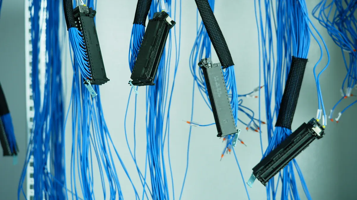
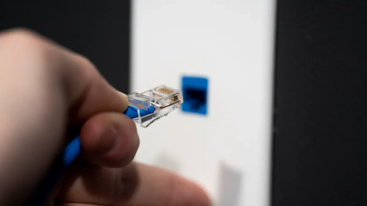
You plug in an ethernet cable, but nothing works. You check the rj45 colour code on both ends and spot something odd. The colors don’t match the standard. Ethernet problems like this can confuse anyone. Always look at the rj45 colour code before connecting a network cable. Use a cable tester to check your ethernet wiring. Remember, wire pairs matter more than matching colors. Grab a reference chart if you need help with ethernet cables.Spotting Non-Standard RJ45 Colour CodeImage Source: pexelsVisual CluesWhen you look at an ethernet cable, you might expect to see the usual t568a color code or t568b color code. Sometimes, though, the rj45 colour code looks different. You may notice stripes, faded colors, or even shades that do not match any standard. If you see wires that look odd, stop and check both ends of the cable.Tip: Always untwist the pairs and lay them flat. This makes it easier to compare the colors to a t568a color code or t568b color code chart.Here are some common signs that you are dealing with a non-standard rj45 color code:The wire colors do not match the t568a color code or t568b color code.Some wires have extra stripes or unusual shades.The order of the colors seems random or mixed up.The cable uses colors not found in standard ethernet cables.You might also run into problems if the cable is old or dirty. Dust and debris inside the connector can make it hard to see the true colors. Physical damage, like bending or crushing, can also change how the wires look.Pairing and ShadesYou may feel tempted to match colors from end to end, but the real key is correct pairing. Technical experts agree that keeping the right pairs together is what keeps your ethernet working well. If you mix up the pairs, your network cable may not work at all, even if the colors look right.A quick table can help you compare standard pairings:Pin Numbert568a color codet568b color code1Green/WhiteOrange/White2GreenOrange3Orange/WhiteGreen/White4BlueBlue5Blue/WhiteBlue/White6OrangeGreen7Brown/WhiteBrown/White8BrownBrownIf you see a cable that does not follow these patterns, check the pairs by untwisting and matching them up. Sometimes, you will find that the cable uses the right pairs but with different colors. That is okay, as long as the pairs match at both ends.You may also run into trouble if the cable is not the right type for your needs. Using a Cat5 cable instead of Cat6 can slow down your ethernet or cause problems with high-speed connections. Improper crimping or damaged connectors can also lead to network failures or complete disconnection.Remember: Always focus on correct pairing, not just matching colors. This will help you avoid headaches and keep your ethernet running smoothly.RJ45 Color Code Identification StepsImage Source: pexelsTools NeededBefore you start working with any ethernet cable, you need the right tools. Having the right equipment makes the job easier and helps you avoid mistakes. Here’s what you should have on hand:Cable tester: This device checks if your ethernet cable works and if all wires connect correctly. Some cable testers can even show you which wire is broken or out of order.Multimeter: You can use this tool to check for continuity and make sure there are no shorts in the cable.Reference charts: Keep a chart for the t568b color code and other wiring standards nearby. This helps you compare what you see with what’s correct.Wire stripper: This tool lets you remove the outer jacket of the cable without damaging the wires inside.Crimping tool: You need this to attach a new rj45 connector if you have to re-terminate the cable.Flashlight: Sometimes, you need extra light to see the wire colors clearly.Tip: Good lighting and a clean workspace help you spot color differences and avoid mixing up wires.Many cable testers offer advanced features. Some can measure cable length, check for signal loss, and even test for Power over Ethernet (PoE). Others use LEDs to show if each wire connects properly. Testing devices like the Fluke LinkIQ can diagnose problems like crosstalk or signal loss. These features help you find and fix issues fast.Mapping WiresNow, let’s get into the process of mapping the wires. This step is where you match each wire to its correct pin in the rj45 connector. You want to make sure the cable works for ethernet, even if the rj45 color code looks different from what you expect.Strip about one inch of the cable’s outer jacket. Be careful not to nick the wires inside.Untwist the wire pairs and straighten them out. Lay them flat so you can see all the colors.Compare the wire colors to your reference chart. Even if the colors are odd, focus on keeping the pairs together.Arrange the wires in the order you want for the rj45 connector. Use either the T568A or T568B standard, but stay consistent at both ends.Trim the wires so they are even. This helps them fit into the connector.Insert the wires into the rj45 connector. Double-check the order before you crimp.Use your crimping tool to secure the connector.Test the cable with your cable tester. Make sure each pin connects to the right spot at the other end.Note: Always check both ends of the cable. The pinout must match for ethernet to work. If you see a non-standard rj45 color code, write down the order for future reference.Industry standards like T568A and T568B, set by the Telecommunications Industry Association (TIA) and Electronic Industries Alliance (EIA), define how you should map wire colors to pin numbers. These standards help everyone create cables that work with all devices. The IEEE 802.3 Ethernet standard also explains which pins send and receive data. Following these steps and standards keeps your network stable and fast.Custom DiagramWhen you run into a non-standard rj45 color code, drawing your own diagram can save you time later. A custom diagram shows exactly how the wires connect inside the rj45 connector. This is helpful if you need to fix the cable again or explain the wiring to someone else.Here’s a simple way to make your own diagram:Pin NumberWire Color at End AWire Color at End B12345678Fill in the table with the actual colors you see at each end of the ethernet cable. If the colors do not match the t568b color code or any standard, this table helps you keep track. You can also take a photo of the cable ends for your records.Pro Tip: Save your diagram or photo with the cable or in your network documentation. This makes troubleshooting much easier if you or someone else needs to check the cable later.Technical guides recommend documenting your custom wiring, especially for non-standard setups. This helps you avoid confusion and keeps your network running smoothly. Consistency and clear records are key when working with any rj45 connector.RJ45 Connector TroubleshootingContinuity TestingWhen your ethernet cable stops working, you need to check if the wires inside connect the right way. That’s where a cable tester comes in handy. You plug both ends of the cable into the tester. The device checks if each wire goes from one end to the other without any breaks or shorts. This is called a continuity test.A continuity test is the first step in finding problems with an rj45 connector. If the tester shows a problem, you know there is a break or a short inside the cable. Sometimes, the tester will show that all wires connect, but your ethernet still does not work. This can happen if the pairs are mixed up or twisted the wrong way. In that case, you may need more advanced testing devices or a loopback test. A loopback test sends a signal through the cable and checks if it comes back. This helps you find deeper problems like signal loss or poor connections.Tip: Always start with a continuity test. If you still have trouble, try a loopback test or check the cable with a different device.Some advanced testers also measure resistance and signal quality. They can tell you if the cable can carry data at high speeds. These extra tests help you find problems that a simple continuity test might miss.Common IssuesYou might run into several problems when working with an rj45 connector. Here are some of the most common issues:Mismatched pairs: The wires are not paired correctly. This can cause slow speeds or no connection at all.Split pairs: The wires from different pairs get mixed up. Your ethernet might pass a basic test but still fail to work right.Shorts and opens: A short means two wires touch when they should not. An open means a wire does not connect at all.Intermittent connections: Sometimes the cable works, and sometimes it does not. This can happen if the wires do not fit tightly in the connector.Physical damage: Bent pins, crushed cables, or worn-out connectors can all cause trouble.Technical reports show that even small differences in wire thickness can cause problems. For example, if the wires are too thin, they might not fit the rj45 connector well. This can lead to loose connections, especially at higher speeds or when using Power over Ethernet. Always check that your cable and connector match in size.Note: Using certified cables and connectors helps you avoid many of these problems. Always follow the wiring standards like T568A or T568B.If you keep running into the same problems, you might need to look at your installation process. Make sure you do not untwist the pairs too much. Only expose about one inch of wire when you strip the cable. This keeps the signal strong and reduces errors.Fixing and Re-TerminationIf you find a problem with your rj45 connector, you can often fix it by re-terminating the cable. Here’s how you can do it:Cut off the old connector with a clean snip.Strip about one inch of the cable jacket. Be careful not to damage the wires inside.Untwist the pairs just enough to fit them into the connector. Keep the twists as close as possible to the connector.Arrange the wires in the correct order for T568A or T568B.Trim the wires so they are even.Insert the wires into a new rj45 connector.Use a crimping tool to secure the connector.Test the cable again with your cable tester.Some new systems, like the REVConnect, make this process even easier. They use a special tool and a universal cable manager. You do not need to untwist the pairs as much, which keeps the signal strong. Even if you do not have special tools, you can still get good results by following the steps above.Pro Tip: Always test the cable after you fix it. If you still have trouble, check your work or try a new connector.Best practices say you should always follow industry standards when you repair or re-terminate a cable. Use the right tools, keep your workspace clean, and document your work. This helps you and others fix problems faster in the future.If you see the same issue again and again, check your cables and connectors. Make sure they are certified and match in size. Sometimes, the problem is not with your work but with the parts you use.Network Cable DocumentationLabeling WiresYou can save yourself a lot of trouble by labeling every network cable as soon as you make it. Clear labels on both ends help you know exactly where each cable goes. Use durable labels that won’t fade or fall off. Write down the port number, device name, or even the room location. Some people use color-coded wraps or cables to make things even easier. This helps you spot different network segments at a glance.Pro Tip: Good cable management can cut troubleshooting time by more than half and help your equipment last longer.Many companies use cable management tools like D-Rings, patch panels, or vertical organizers. These tools keep your cables neat and easy to trace. When you label and organize your network cable setup, you avoid confusion and reduce the risk of unplugging the wrong wire. You also make it easier for anyone else who works on your network later.Here’s a quick checklist for labeling:Label both ends of every cable.Include port numbers, device IDs, or destinations.Use color codes for different network segments.Update labels if you move or change cables.Sharing InfoYou should always keep records of your network cable layout. Draw diagrams or use spreadsheets to track where each cable runs and what it connects to. If you make changes, update your records right away. Write down the date, what you changed, and who did the work. This way, you build a history that helps with future upgrades or repairs.When you work with other technicians, share your documentation. Clear records help everyone understand the setup. If you use special color codes or non-standard wiring, make sure to explain them. Good documentation and communication can prevent mistakes and keep your network running smoothly.Note: Following best practices like labeling, documenting, and sharing info leads to fewer network outages and faster repairs.You can avoid network headaches by always checking, testing, and writing down any non-standard RJ45 color codes you find. Make sure the wire pairs match at both ends. Use the right tools and keep your notes handy. Studies show that when you follow these steps, you get:Fewer network failures and less downtimeFaster troubleshooting and easier repairsStronger, more reliable connectionsStay organized and share your documentation. Your network will thank you! ??FAQWhat should you do if the wire colors don’t match any standard?If you see strange colors, stop and check both ends of the cable. Use a cable tester. Focus on keeping the wire pairs together. Write down the color order for future reference.Can you use a cable with non-standard colors for Ethernet?Yes, you can. The cable will work if the pairs match at both ends. The color does not matter as much as the correct pairing. Always test the cable before using it.How do you fix a cable with mixed-up pairs?Cut off the connector. Arrange the wires in the right order for T568A or T568B. Crimp a new connector. Test the cable again. This usually solves the problem.Why is documenting non-standard wiring important?You might forget the color order later. Good documentation helps you and others fix or replace cables quickly. It also prevents mistakes during future repairs.What tools help you identify non-standard RJ45 color codes?Cable testerReference chartFlashlightMultimeterThese tools make it easier to spot problems and fix them fast.
On 2025-08-16