Choosing the right FPGA can transform your application by improving performance, reducing costs, and boosting efficiency. For instance, FPGAs excel in energy efficiency, with up to 30% lower power dissipation in vision-based machine learning tasks compared to CPUs or GPUs. This reduces thermal management needs and enhances system reliability. Their dynamic reconfiguration capability also allows real-time hardware adjustments, ensuring optimal performance under varying conditions. Furthermore, the deterministic latency of FPGAs, measured in nanoseconds, makes them ideal for precise tasks like encryption or network synchronization. Selecting an FPGA like the XCKU085-2FLVA1517I with the right features ensures you meet your design goals effectively.
Understanding Your Application Needs
Define Project Goals and Objectives
Before selecting an FPGA, you need to clearly define your project’s goals. Ask yourself what you aim to achieve with your design. Are you building a high-speed data processing system, or do you need a low-power solution for an embedded application? Identifying these objectives helps you narrow down your options and focus on FPGAs that align with your needs.
The FPGA market offers a wide range of technologies, each suited to different applications. This diversity allows industries like telecommunications, automotive, and healthcare to benefit from the adaptability of FPGAs. By understanding your goals, you can choose a solution tailored to your specific requirements.
Tip: Write down your project’s primary objectives and rank them by importance. This will help you prioritize features when evaluating FPGA options.
Evaluate Performance and Processing Requirements
Performance is a critical factor in FPGA selection. You need to evaluate the processing power and logic resources required for your design. For example, if your project involves high-speed data transfer, selecting an FPGA with the right I/O interface is essential. Factors like data rate, power consumption, and noise immunity play a significant role in ensuring your design meets performance expectations.
Modern FPGAs offer advanced features like high-speed SERDES interfaces and DSP blocks, which enhance processing capabilities. However, these features come at a cost. Balancing performance with budget constraints is key to making an informed decision.
Note: Choosing an FPGA with more resources than you need can increase costs unnecessarily. Focus on finding a balance between performance and value.
Consider Environmental and Operational Constraints
Environmental and operational conditions can significantly impact FPGA performance. For instance, if your design will operate in harsh environments, you need an FPGA that can withstand extreme temperatures and vibrations. Similarly, operational constraints like power availability and thermal management must be considered.
Research shows that FPGAs experience gradual degradation in switching frequency over time. This highlights the importance of predictive maintenance, especially for critical systems. By understanding these constraints, you can plan for future challenges and ensure long-term reliability.
Additionally, optimizing resource utilization is crucial in FPGA design. Advanced synthesis techniques can help you overcome resource limitations, enhancing productivity and innovation.
Tip: Always check the FPGA’s datasheet for environmental specifications and operational limits before making a decision.
Assess Budget and Cost Limitations
Budget plays a crucial role in selecting the right FPGA for your design. You need to carefully evaluate how much you can allocate to the project without compromising on essential features. A well-planned budget ensures that you achieve your design goals while staying within financial limits.
Understand the Breakdown of Costs
When planning your budget, it’s important to understand the different cost components involved in FPGA selection. These include material costs, development tools, and personnel expenses. Personnel costs often make up a significant portion of the total budget, especially during the prototyping phase. Overlooking these costs can lead to unexpected financial challenges.
Here’s a breakdown of common cost components to consider:
Cost Component
Description
Personnel Cost
A significant portion of the prototyping project, often larger than material cost differences.
A tool developed to input important cost components and provide a comprehensive cost overview.
Real Costs
Understanding these costs is crucial for making informed decisions regarding FPGA selection.
Using tools like a Cost Comparison Spreadsheet (CCS) can help you analyze these components effectively. This approach provides a clear picture of where your money is going and helps you identify areas where you can save.
Balance Cost with Performance
While it might be tempting to choose the cheapest FPGA available, this approach can backfire. Low-cost options often lack the advanced features or processing power required for complex designs. On the other hand, high-end FPGAs may exceed your needs and inflate your budget unnecessarily. Striking the right balance between cost and performance is key.
For example, if your design requires high-speed data processing, investing in an FPGA with sufficient logic resources and interfaces is essential. However, if your application is less demanding, a mid-range FPGA might offer better value for money. Always match the FPGA’s capabilities to your project’s requirements to avoid overspending.
Tip: Avoid overestimating your needs. Choose an FPGA that meets your current requirements but allows room for minor upgrades.
Plan for Hidden Costs
Hidden costs can significantly impact your budget. These include expenses for development tools, software licenses, and evaluation boards. Additionally, consider the cost of training your team to work with the selected FPGA. These factors often go unnoticed during the initial planning phase but can add up quickly.
To avoid surprises, create a detailed budget that accounts for all potential expenses. Include a buffer for unexpected costs to ensure your project stays on track.
Leverage Cost-Effective Solutions
Many manufacturers offer cost-effective solutions for FPGA development. These include free or low-cost development tools, open-source resources, and community support. Taking advantage of these options can reduce your overall expenses without compromising on quality.
Additionally, consider using evaluation boards to test your design before committing to a specific FPGA. This approach minimizes the risk of costly mistakes and ensures that the chosen FPGA meets your expectations.
Note: Investing in a slightly higher-cost FPGA with better support and documentation can save you money in the long run by reducing development time and errors.
By carefully assessing your budget and understanding the associated costs, you can make an informed decision that aligns with your financial and design goals.
The FPGA package plays a critical role in determining how well the device integrates into your design. Packages come in various types and sizes, each suited to specific applications. For instance, Ball Grid Array (BGA) packages offer high pin density, making them ideal for compact designs. On the other hand, Quad Flat Packages (QFP) provide easier soldering and inspection, which can simplify prototyping.
When evaluating an FPGA package, consider the number of pins, thermal performance, and physical dimensions. A smaller package might save space but could limit the number of available I/O pins. Conversely, a larger package may offer more connectivity options but increase the overall size of your design.
Tip: Always match the FPGA package to your PCB layout and manufacturing capabilities. This ensures compatibility and reduces production challenges.
Logic Resources and Processing Power
Logic resources and processing power define the computational capabilities of an FPGA. These features determine how efficiently the FPGA can handle your design's workload. Modern FPGAs include configurable logic blocks (CLBs), digital signal processing (DSP) slices, and embedded memory to support complex operations.
To evaluate processing power, you can refer to industry-standard benchmarks. For example, the PREP Benchmark Suite measures average benchmark capacity and speed, while the Toronto 20 Benchmark evaluates area-delay product metrics. The LINPAC Benchmark focuses on floating-point execution rates, providing insights into the FPGA's performance in mathematical computations.
Benchmark Suite
Description
Key Metrics
PREP Benchmark Suite
Demonstrates performance and capacity of programmable logic devices.
Average Benchmark Capacity (ABC), Average Benchmark Speed (ABS)
Toronto 20 Benchmark
Originated from an FPGA place-and-route challenge to benchmark software tools.
Area ratios, area-delay product evaluation metric
LINPAC Benchmark
Contains FORTRAN subroutines for solving linear equations.
Floating-point rate of execution (Mflops/s), theoretical peak performance
Selecting an FPGA with sufficient logic resources ensures your design can meet its performance goals. However, overestimating your needs can lead to unnecessary costs.
Note: Choose an FPGA that balances processing power with your application's complexity. This approach optimizes both performance and cost.
Interfaces and Connectivity (e.g., SERDES, LVDS, GPIO)
Interfaces and connectivity options are vital for ensuring seamless communication between the FPGA and other components in your system. High-speed interfaces like SERDES (Serializer/Deserializer) enable efficient data transfer, making them essential for applications like video processing and high-frequency trading. Similarly, LVDS (Low-Voltage Differential Signaling) provides noise-resistant communication, ideal for automotive and industrial environments. General-purpose I/O (GPIO) pins offer flexibility for connecting to various peripherals.
When evaluating these interfaces, consider the technical standards and reliability metrics they must meet. For example, in automotive systems, interfaces often need to comply with ISO 26262 functional safety requirements. Designers face challenges in selecting I/O libraries that ensure reliability and quality. These considerations apply to other interfaces as well, such as SERDES and LVDS, where maintaining signal integrity and minimizing latency are critical.
Tip: Review the FPGA's datasheet to confirm the availability and specifications of the required interfaces. This step ensures compatibility with your system's communication protocols.
Power Consumption and Efficiency
Power consumption is a critical factor when selecting an FPGA for your design. Efficient power usage not only reduces operational costs but also minimizes heat generation, which can improve the reliability of your system. Modern FPGAs incorporate several techniques to optimize power efficiency, ensuring they meet the demands of various applications.
Dynamic Voltage and Frequency Scaling (DVFS): This technique adjusts the voltage and frequency of the FPGA based on workload requirements. By lowering these parameters during less intensive tasks, you can achieve significant power savings.
Thermal Management: Effective thermal management, such as using heat sinks or cooling systems, enhances power efficiency. It prevents overheating, which can degrade performance and shorten the lifespan of your FPGA.
Power Profiling: Profiling power consumption under different conditions helps you identify hotspots in your design. This allows you to optimize the FPGA's configuration for better power usage.
To understand power consumption in detail, consider the three main components:
Dynamic Power: This depends on switching activity and is calculated using the formula: Pdynamic = α?C?V2?f. Reducing the switching activity or voltage can lower dynamic power.
Static Power: This is the power consumed when the FPGA is idle. It is influenced by leakage current and can be expressed as Pstatic = Ileakage?V.
I/O Power: This is associated with active input/output pins. The number of pins and their driving strength directly impact this component.
Tip: Use power profiling tools provided by FPGA manufacturers to monitor and optimize power consumption in real-time. This ensures your design remains efficient under varying workloads.
Cost and Value for Money
Balancing cost and value is essential when choosing an FPGA. While it might be tempting to select the cheapest option, you should focus on the overall value the FPGA brings to your design. A cost-effective FPGA offers the right combination of features, performance, and support without exceeding your budget.
Factors Influencing Cost
FPGA Package: The type and size of the FPGA package can significantly affect its cost. For example, a Ball Grid Array (BGA) package may cost more due to its higher pin density and compact design. However, it provides better integration for complex systems.
Performance Needs: High-performance FPGAs with advanced features like DSP blocks or high-speed interfaces often come at a premium. If your design doesn't require these features, opting for a mid-range FPGA can save costs.
Development Tools and Support: Some manufacturers offer free or low-cost development tools, which can reduce overall expenses. Additionally, FPGAs with extensive documentation and community support can lower development time and costs.
Maximizing Value
To get the best value for your investment, consider the following:
Choose an FPGA that meets your current requirements but allows for future upgrades. This ensures scalability without the need for a complete redesign.
Evaluate the total cost of ownership, including development tools, training, and maintenance. Sometimes, a slightly more expensive FPGA with better support can save money in the long run.
Use evaluation boards to test your design before committing to a specific FPGA. This minimizes the risk of costly mistakes.
Note: Always compare the cost of different FPGAs against their features and performance. This helps you identify the option that offers the best value for your application.
Advanced Features (e.g., read/write leveling circuitry)
Advanced features in FPGAs can significantly enhance their functionality and performance. One such feature is read/write leveling circuitry, which is crucial for designs involving high-speed memory interfaces like DDR3.
In DDR3 DIMM designs, write leveling ensures proper synchronization between the data strobe (DQS) and data signals (DQ). This is achieved through programmable circuits that adjust the skew of these signals. By aligning them correctly, you can maintain data integrity and achieve reliable communication.
The alignment and synchronization block in FPGAs plays a vital role in read/write leveling. It ensures compatibility with JEDEC-compliant DDR3 DIMMs, which is essential for high-speed operations. Additionally, the calibration control block enhances timing margins during the resynchronization stage. This block uses a deskew algorithm to improve timing accuracy, surpassing traditional static timing methods.
For example, the Virtex-5 FPGA includes IDDR registers that capture data inputs. These registers allow for programmable delays of incoming strobe and data signals. This ensures the clocking signal aligns with the valid data window, which is critical for reliable data transmission.
Tip: If your design involves high-speed memory interfaces, prioritize FPGAs with advanced features like read/write leveling circuitry. These features simplify implementation and improve performance.
Peripheral and connector support determines how well an FPGA board integrates with external devices. You need to evaluate the available connectors and interfaces to ensure compatibility with your design. For example, boards with industry-standard connectors like PCIe or USB simplify integration with existing systems. GPIO pins provide flexibility for connecting sensors, actuators, or other peripherals.
Modern FPGA boards often include high-speed connectors for applications requiring fast data transfer. These connectors reduce latency and improve communication efficiency. Boards designed for NVMe technology, such as the 250 series FPGA boards, offer low-latency access to storage, making them ideal for data-intensive applications.
Tip: Choose an FPGA board with connectors that match your system requirements. This minimizes setup complexity and ensures reliable operation.
Assess Memory and Storage Options
Memory and storage capabilities play a crucial role in FPGA board performance. Boards with sufficient memory ensure smooth operation for complex designs. For instance, the Intel? Stratix? 10 GX FPGA supports up to 8 GB DDR4 memory per socket, with ECC for error correction. This configuration suits applications requiring high-speed data processing and reliability.
Here’s a breakdown of memory specifications for a typical FPGA board:
Feature
Description
FPGA
Intel? Stratix? 10 GX FPGA
Memory
128 MB FLASH, 4 independent DDR4 SO-DIMM sockets with ECC, up to 8 GB 1200 MHz
Recent FPGA families also include embedded low-power microprocessors, enhancing efficiency. Products based on NVMe technology reduce I/O bottlenecks, improving data access speed.
Note: Select an FPGA board with memory options that align with your application’s data processing needs. This ensures optimal performance without overspending.
Prioritize Ease of Use and Development Tools
Ease of use is a critical factor when choosing an FPGA board. Boards with user-friendly interfaces and stable programming tools simplify development. High-quality documentation helps you understand the board’s features and reduces setup time. Avoid boards with excessive jumper settings, as they complicate initial configuration.
Manufacturers often differentiate their products through ease of use. Boards with intuitive design and robust development tools enhance productivity. For example, user-friendly programming environments reduce errors and speed up prototyping.
Tip: Look for FPGA boards with comprehensive documentation and straightforward setup processes. This saves time and ensures a smoother development experience.
Verify Compatibility with xcku085-2flva1517i
Ensuring compatibility with the xcku085-2flva1517i is a crucial step in your FPGA selection process. This specific FPGA offers advanced features, but you need to confirm that it aligns with your design requirements and system architecture.
Start by reviewing the datasheet for the xcku085-2flva1517i. Pay close attention to its pin configuration, power requirements, and supported interfaces. These details help you determine if the FPGA can integrate seamlessly into your design. For example, if your project involves high-speed data transfer, verify that the xcku085-2flva1517i supports the necessary SERDES or LVDS interfaces.
Next, evaluate the development tools and software compatibility. The xcku085-2flva1517i works best with specific design tools provided by the manufacturer. Ensure that your team has access to these tools and understands how to use them effectively. This step minimizes development time and reduces the risk of errors.
You should also consider the physical compatibility of the xcku085-2flva1517i with your PCB layout. Check the package type and size to confirm that it fits within your board's design constraints. If your project involves tight space limitations, this FPGA's package options might influence your decision.
Finally, test the xcku085-2flva1517i using an evaluation board. This allows you to validate its performance and compatibility before committing to full-scale production. Testing ensures that the FPGA meets your expectations and functions as intended in your application.
Tip: Always cross-check your design's requirements with the xcku085-2flva1517i's specifications. This ensures a smooth integration process and avoids costly redesigns.
Additional Considerations
Customization and Scalability
Customization and scalability are two of the most powerful advantages of FPGA designs. You can tailor an FPGA to meet your specific project requirements, ensuring it performs optimally for your application. This flexibility allows you to adapt your design as your needs evolve, making FPGAs a future-proof solution.
The NI cRIO platform enabled the creation of a custom C Series module for signal conversion. This approach improved system maintainability and allowed for easier updates.
These examples highlight how FPGAs can transform industries by offering unmatched flexibility and scalability. By leveraging these features, you can ensure your design remains relevant and efficient over time.
Availability of Documentation and Tutorials
Comprehensive documentation and tutorials are essential for a smooth FPGA development process. They provide step-by-step guidance, helping you understand the FPGA's capabilities and how to implement them effectively. Manufacturers like Intel and Altera offer detailed how-to guides, updates, and training programs to support their FPGA products.
Access to tutorials and training videos can significantly reduce the learning curve for new developers. For instance, Altera engineers have created a library of how-to videos that cover various aspects of FPGA design. These resources not only save time but also help you avoid common mistakes during development.
When selecting an FPGA, always check the availability of documentation and tutorials. A well-documented product ensures you can quickly resolve issues and make the most of your FPGA's potential.
Manufacturer Support and Community Resources
Strong manufacturer support and active community resources can make a significant difference in your FPGA development experience. Leading manufacturers provide a range of support options, including developer forums, evaluation boards, and software tools like Vivado and Vitis. These resources help you troubleshoot problems and enhance your design.
Here’s a quick overview of what top manufacturers offer:
Resource Type
Description
Documentation
Step-by-step guides and updates for resolving issues.
Community Support
Access to forums where you can discuss challenges with experts and other developers.
Training Programs
Tutorials and videos created by FPGA engineers to improve your skills.
Quality Assurance
Commitment to delivering reliable and high-quality FPGA products.
By engaging with these resources, you can gain valuable insights and stay updated on the latest advancements in FPGA technology. A strong support network ensures you have the tools and knowledge needed to succeed in your project.
Longevity and Future-Proofing
When selecting an FPGA, you should consider its longevity and ability to adapt to future needs. Technology evolves rapidly, and choosing an FPGA that can keep up with these changes ensures your design remains relevant for years. Manufacturers often release lifecycle and upgrade reports to help you assess the long-term viability of their products. These reports provide insights into how long the FPGA will remain supported and whether it can handle emerging technologies like post-quantum cryptography (PQC).
To enhance longevity, many FPGAs now include modular designs. These allow you to upgrade specific components without replacing the entire device. For example:
Modular FPGAs can adapt to new PQC requirements, reducing the need for complete redesigns.
Recyclable materials and partnerships with certified recycling providers minimize e-waste when hardware becomes obsolete.
By prioritizing these features, you can future-proof your design while contributing to sustainability. Always review the FPGA's roadmap and upgrade options to ensure it aligns with your long-term goals.
Tip: Look for FPGAs with a proven track record of updates and support. This guarantees compatibility with future technologies and reduces the risk of early obsolescence.
Availability of Evaluation Boards
Evaluation boards play a crucial role in FPGA development. These boards let you test your design before committing to full-scale production. By using an evaluation board, you can verify the FPGA's performance, debug potential issues, and optimize your design for efficiency.
Most manufacturers offer evaluation boards tailored to their FPGA families. These boards often include pre-configured interfaces, memory modules, and connectors, making it easier to prototype your application. For instance, some boards feature high-speed interfaces like PCIe or Ethernet, which are essential for data-intensive projects. Others provide GPIO pins for simpler designs.
When choosing an evaluation board, ensure it matches your FPGA's specifications. Check for compatibility with your design tools and confirm that the board includes the peripherals you need. Testing your design on an evaluation board reduces the risk of costly mistakes and accelerates development.
Note: Investing in a high-quality evaluation board can save time and resources during the prototyping phase. It also helps you identify potential challenges early in the process.
Selecting the right FPGA for your application requires careful consideration of multiple factors. Performance, cost, and scalability play pivotal roles in ensuring your design meets its objectives. For instance, FPGAs excel in parallelism and rapid prototyping, enabling efficient testing and iteration. However, they may not match ASICs in speed for certain tasks or microcontrollers in cost-effectiveness for high-volume production.
Factor
Description
Performance
FPGAs deliver high performance but may lag behind ASICs in specific applications.
Cost
Typically more expensive than microcontrollers or ASICs, especially in large-scale production.
Scalability
Designs can be adjusted to meet varying requirements, optimizing resource use.
Flexibility
Reprogrammable for diverse functions, making them versatile for different applications.
Rapid Prototyping
Enables quick testing and iteration, reducing time-to-market for new designs.
Adopting a structured approach simplifies decision-making. Evaluate package selection, resource requirements, and customization options to align the FPGA with your project needs. Comprehensive documentation and quality support further enhance confidence and efficiency during implementation.
Tip: A methodical framework ensures you balance technical requirements with practical constraints, paving the way for a successful design.
FAQ
What is the most important factor when choosing an FPGA?
You should prioritize your application’s requirements. Focus on performance, logic resources, and connectivity options. These factors ensure the FPGA aligns with your design goals. Always balance these needs with your budget to avoid overspending.
How do I determine if an FPGA meets my power requirements?
Check the datasheet for power consumption details. Look for features like dynamic voltage scaling and thermal management. Use power profiling tools to estimate real-world usage. This ensures your design remains efficient under different workloads.
Can I upgrade my FPGA design later?
Yes, FPGAs are reprogrammable. You can modify your design to add new features or improve performance. Choose an FPGA with extra resources to allow for future upgrades without needing a complete redesign.
Are evaluation boards necessary for FPGA development?
Evaluation boards simplify testing and debugging. They let you validate your design before production. This reduces risks and saves time. Always choose a board compatible with your FPGA and project requirements.
How do I find support if I face issues during development?
Manufacturers provide documentation, forums, and training resources. Join online communities to connect with other developers. These platforms help you troubleshoot problems and learn best practices for FPGA design.
XCKU085-2FLVA1517I Documents & Media
Download datasheets and manufacturer documentation for Xilinx Inc. XCKU085-2FLVA1517I.
Kynix was founded in 2008, specializing in the electronic components distribution business. We adhere to honesty and ethics as our business philosophy and have gradually established an excellent reputation and credibility in our international business. With the accurate quotation, excellent credit, reasonable price, reliable quality, fast delivery, and authentic service, we have won the praise of the majority of customers.
Join our mailing list!
Be the first to know about new
products, special offers, and
more.
Quick-Reference Card: AD8594 at a GlanceAttributeDetailComponent TypeQuad Operational Amplifier (CMOS, Rail-to-Rail I/O)ManufacturerAnalog Devices, Inc.Key Spec±250 mA High Output CurrentSupply Voltage2.5 V to 6 VPackage OptionsSOIC, TSSOP (Refer to datasheet)Lifecycle StatusActiveBest ForMobile communication handset audio and PC line driving1. What Is the AD8594? (Definition + Architecture)The AD8594 is a quad CMOS single-supply, rail-to-rail input/output operational amplifier from Analog Devices, Inc. that delivers a massive ±250 mA output current while featuring an ultra-low 100 nA shutdown mode. Unlike standard general-purpose op-amps that struggle to drive heavy loads, the AD8594 is explicitly designed to act as a robust line driver without requiring a secondary buffer stage.1.1 Core Architecture & Design PhilosophyInternally, the AD8594 leverages a CMOS architecture optimized for low-voltage, single-supply operation. The manufacturer prioritized current drive capability and power efficiency. By incorporating a true rail-to-rail input and output (RRIO) structure, the device maximizes dynamic range even on a constrained 2.5V or 3.3V supply. The addition of a dedicated shutdown pin allows designers to aggressively power-gate the IC, dropping consumption to near zero when the signal path is inactive.1.2 Where It Fits in the Signal Chain / Power PathThe AD8594 typically sits at the very end of the analog signal chain. It is driven by downstream DACs, audio codecs, or ASIC outputs, and it directly interfaces with heavy physical loads—such as headphones, LCD reference planes, or long cable lines. Because it is unity-gain stable, it is frequently configured as a heavy-duty voltage follower.2. Electrical Characteristics: The Numbers That Matter2.1 Power Supply & Consumption ProfileSupply Voltage Range: 2.5 V to 6 V. Why it matters: This part thrives on modern 3.3V and 5V logic rails, but it cannot be used in legacy ±15V or standard 12V industrial systems.Supply Current: 750 μA per amplifier. Why it matters: For a device capable of pushing 250 mA, a sub-1mA quiescent current per channel is highly efficient, extending battery life in portable instrumentation.Shutdown Current: 100 nA. Why it matters: This effectively removes the op-amp from the battery budget when the device is asleep, making external load switches unnecessary.2.2 Performance Specs (Speed, Accuracy, or Efficiency)Output Current: ±250 mA. Why it matters: This is the standout spec. It eliminates the need for discrete push-pull transistor buffers when driving low-impedance loads like speakers or long coaxial cables.Gain Bandwidth Product (GBW): 3 MHz. Why it matters: This provides plenty of headroom for high-fidelity audio frequencies and standard data acquisition (DAQ) sampling rates without introducing phase distortion.Slew Rate: 5 V/μs. Why it matters: Ensures the amplifier can faithfully track fast-changing signals, preventing slew-induced distortion in high-amplitude PC audio lines.No Phase Reversal: Why it matters: If the input signal accidentally exceeds the supply rails, the output won't violently invert polarity—a critical safety feature in unpredictable sensor environments.2.3 Absolute Maximum Ratings — What Will Kill ItMaximum Supply Voltage (6V): Do not exceed 6V. Connecting this to an unregulated 2-cell Li-Po battery (which peaks at 8.4V) will instantly destroy the silicon.Thermal Limits: Pushing ±250 mA continuously across all four channels will exceed the thermal dissipation limits of standard packages. You must calculate junction temperature based on your specific load.3. Pinout & Package Guide3.1 Pin-by-Pin Functional Groups(Note: Pin numbering varies by package. Always consult the AD8594 datasheet for exact mappings.)Pin GroupPinsFunctionPowerVDD, GNDSingle-supply rails (2.5V to 6V)InputsINA+, INA-, INB+, etc.Non-inverting and inverting inputs for all 4 channelsOutputsOUTA, OUTB, OUTC, OUTDHigh-current rail-to-rail outputsControlSHDNActive-low or active-high shutdown (refer to datasheet for logic levels)3.2 Package Variants & Soldering NotesPackagePitchThermal Pad?Soldering MethodSOIC-14/161.27 mmNoStandard reflow / Easy hand-solderingTSSOP-14/160.65 mmNoStandard reflow / Requires flux for hand-soldering(Because this device drives high currents, ensure traces leading to the OUT and VDD/GND pins are wide enough to handle 250mA, and use generous copper pours to assist with passive cooling.)3.3 Part Number DecoderAD8594: Base part number (Quad Op-Amp).A: Temperature grade (-40°C to 85°C).R / RU: Package designator (R = SOIC, RU = TSSOP).Z: RoHS Compliant / Pb-free.4. Known Issues, Errata & Real-World Pain PointsWhy this section exists: Community forums, application notes, and field reports reveal problems the datasheet glosses over. This section saves you hours of debugging.Problem: Thermal Dissipation & Overheating * Root Cause: Driving high output currents (up to 250mA) in small SOIC or TSSOP packages causes significant self-heating ($P = I^2R$). If all four channels drive heavy loads simultaneously, the junction temperature will easily trigger thermal limits. * Recommended Fix: Maximize PCB copper area around the VDD and GND pins for heat sinking. Limit continuous output current, or use duty-cycling to keep the average thermal load within safe operating margins.Problem: Limited Maximum Supply Voltage * Root Cause: The absolute maximum supply voltage is aggressively capped at 6V. * Recommended Fix: It is strictly unsuitable for standard 12V, 15V, or 24V industrial systems. You must use a dedicated 5V or 3.3V LDO regulated rail. If your system requires higher voltages, select a different industrial op-amp.Problem: Input Offset Voltage Limitations * Root Cause: With an offset voltage of up to 2mV, this part prioritizes current drive over DC precision. * Recommended Fix: It may not be suitable for high-precision DC measurement applications (like strain gauges). Implement software calibration in your MCU to null the offset, or choose a zero-drift/precision op-amp for sensitive DC front-ends.5. Application Circuits & Integration Examples5.1 Typical Application: PC Audio Line DrivingIn PC audio or mobile handset applications, the AD8594 is an excellent choice for driving 32-ohm headphones or long line-out cables. Configured as a non-inverting amplifier, the rail-to-rail output ensures maximum volume without clipping on a 3.3V supply. The 3 MHz bandwidth easily covers the 20 Hz – 20 kHz audio spectrum, while the 5 V/μs slew rate prevents transient intermodulation distortion.5.2 Interface Example: Connecting to a MicrocontrollerTo leverage the 100 nA shutdown feature for battery-powered instrumentation, connect the SHDN pin to a GPIO on your MCU (e.g., via STM32 HAL or an Arduino library).// Pseudocode for MCU integration (STM32 HAL example)void init_audio_amplifier(void) { // Configure GPIO for AD8594 Shutdown pin pinMode(SHDN_PIN, OUTPUT); // Put AD8594 to sleep (100nA mode) on boot digitalWrite(SHDN_PIN, LOW); }void play_audio(void) { // Wake up the AD8594 digitalWrite(SHDN_PIN, HIGH); delay(1); // Allow amplifier to stabilize // Start DAC output start_DAC_stream();}6. Alternatives, Replacements & Cross-ReferenceIf the AD8594 is out of stock or you need a slightly different spec profile, consider these alternatives.6.1 Pin-Compatible Drop-In Replacements(Always verify the shutdown pin logic and exact package dimensions before dropping in an equivalent.)Part NumberManufacturerKey DifferenceCompatible?MCP604MicrochipLower bandwidth (2.8 MHz), lower output current?? (Check load)OPA4343Texas Instruments5.5 MHz GBW, slightly lower output drive?TLV4120Texas Instruments2.4 MHz GBW, lower power consumption?? (Check current)6.2 Upgrade Path (Better Performance)If you are designing a next-gen product and need lower offset voltage or higher bandwidth, look at the Microchip MCP6024. It offers a wider 10 MHz bandwidth and lower offset, making it a stronger candidate for precision data acquisition systems.6.3 Cost-Down AlternativesFor high-volume consumer goods where the full ±250mA output isn't strictly necessary, the Texas Instruments OPA4310 provides a cost-effective rail-to-rail alternative with excellent availability.7. Procurement & Supply Chain IntelligenceLifecycle Status: Active. The AD8594 is a mature, widely used component.Typical MOQ & Lead Time: Standard reels typically carry an MOQ of 2,500 units. Lead times hover around 12–16 weeks depending on global fab capacity.BOM Risk Factors: Medium-low. While Analog Devices is the sole manufacturer of the specific AD8594 silicon, the generic quad-RRIO op-amp category has multiple cross-reference alternatives (TI, Microchip) if you can tolerate slight differences in output drive.Recommended Safety Stock: 3–6 months for high-volume audio or PCMCIA applications.Authorized Distributors: Purchase only through authorized channels (e.g., Digi-Key, Mouser, Arrow, Avnet) to avoid counterfeit silicon, which often fails to meet the ±250mA output spec.8. Frequently Asked QuestionsQ: What is the AD8594 used for? The AD8594 is primarily used for mobile communication handset audio, PC audio line driving, battery-powered instrumentation, and LCD display reference level drivers due to its high output current.Q: What are the best alternatives to the AD8594? Strong alternatives include the Microchip MCP604 and MCP6024, as well as the Texas Instruments OPA4343 and TLV4120. Selection depends on whether you prioritize bandwidth or output current.Q: Is the AD8594 still in production? Yes, the AD8594 is currently an active component in the Analog Devices portfolio with no immediate End-of-Life (EOL) or Not Recommended for New Designs (NRND) warnings.Q: Can the AD8594 work with 3.3V logic? Yes. The AD8594 operates on a single supply ranging from 2.5V to 6V, making it perfectly suited for modern 3.3V microcontroller and logic systems.Q: Where can I find the AD8594 datasheet and evaluation board? The official AD8594 datasheet and associated evaluation board documentation can be downloaded directly from the Analog Devices, Inc. website or through major authorized electronic component distributors.9. Resources & ToolsOfficial Datasheet: [Analog Devices, Inc. Product Page]Evaluation / Development Kit: Universal Quad Op-Amp Evaluation Boards (available from ADI)Reference Designs: Search for "Analog Devices Audio Line Driver Application Notes"Community Libraries: Compatible with standard STM32 HAL and Arduino digital GPIO control for the shutdown pin.SPICE / LTspice Model: Download the AD8594 .cir or LTspice model from the Analog Devices design center to simulate thermal dissipation and output drive under load.
Quick-Reference Card: S32K118 at a GlanceAttributeDetailComponent Type32-bit Automotive Microcontroller (MCU)ManufacturerNXP USA Inc.Key SpecArm Cortex-M0+ @ 48 MHz with Hardware Security (CSEc)Supply VoltageRefer to official datasheet for exact operating rangesPackage Options48-LQFP (7x7 mm)Lifecycle StatusActive (AEC-Q100 Qualified)Best ForGeneral-purpose automotive body electronics and CAN/LIN nodes1. What Is the S32K118? (Definition + Architecture)The S32K118 is a scalable, AEC-Q100 qualified 32-bit Arm Cortex-M0+ based microcontroller from NXP USA Inc. that delivers robust CAN FD communication and cryptographic security for automotive and industrial systems. While many entry-level MCUs struggle with modern automotive network demands, the S32K118 bridges the gap by pairing a power-efficient M0+ core with advanced peripherals typically reserved for higher-end processors.1.1 Core Architecture & Design PhilosophyAt its heart, the S32K118 runs at up to 48 MHz and is equipped with 256 KB of Flash memory and 25 KB of SRAM. NXP designed this chip with future-proofing in mind. The inclusion of the Cryptographic Services Engine (CSEc) ensures SHE-compliant security, which is now a hard requirement for modern automotive networks to prevent spoofing. Furthermore, the FlexIO module provides a highly configurable state machine capable of emulating additional UART, I2C, SPI, or custom protocols like ISELED, giving designers an "escape hatch" when standard peripherals run out.1.2 Where It Fits in the Signal Chain / Power PathIn a vehicle architecture, the S32K118 typically serves as an edge node or local controller. It sits downstream from the central vehicle gateway, ingesting analog or digital signals from local sensors (e.g., steering angle, temperature, switch states), processing the logic, and driving local actuators (like BLDC motors or HVAC flaps). It then reports system status upstream via its high-speed CAN FD or LIN interfaces.2. Electrical Characteristics: The Numbers That MatterWhen designing with the S32K118, the raw numbers only tell half the story. Here is how the key specifications impact your PCB design and firmware architecture.2.1 Power Supply & Consumption ProfileBecause this is an automotive-grade MCU, it is designed to survive harsh electrical environments, but power sequencing is critical. The device relies on specific power-up timing. If your power supply allows voltage to reach the I/O pins before the core processor is fully powered and stabilized, you risk logic corruption. Always design your power tree to ensure the MCU supply rails are fully established before external communication lines (like CAN transceivers) drive the MCU's pins. Refer to the datasheet for precise voltage thresholds and ramp rates.2.2 Performance Specs (Speed, Accuracy, or Efficiency)The 48 MHz maximum clock frequency is plenty for body electronics, but it requires efficient code. The 256 KB Flash and 25 KB SRAM footprint is generous for an M0+, but firmware engineers must be mindful of SRAM usage when utilizing RTOS queues or large CAN FD message buffers. The integration of CAN FD allows for payload sizes up to 64 bytes at higher bit rates, significantly reducing bus load compared to classical CAN.2.3 Absolute Maximum Ratings — What Will Kill ItI/O Pin Overvoltage During Power-Up: This is the most common killer of the S32K118 in prototype phases. Violating the I/O pin voltage specifications while the MCU is unpowered or transitioning can cause latch-up, flash corruption, or permanent damage. Never allow external devices to back-drive the MCU pins.3. Pinout & Package Guide3.1 Pin-by-Pin Functional GroupsPin GroupPinsFunctionPowerVDD, VSSCore and I/O supply railsCommunicationTX/RXCAN FD, LIN, and UART interfacesFlexIOFXIO_D*Emulated protocols and ISELED controlProgrammingSWDSerial Wire Debug interface3.2 Package Variants & Soldering NotesPackagePitchThermal Pad?Soldering Method48-LQFP0.5 mmNoStandard Reflow / Hand-solderableThe 48-LQFP (7x7 mm) package is excellent for prototyping. The 0.5 mm pitch is forgiving enough for hand-soldering during the bring-up phase, and the lack of an exposed thermal pad simplifies routing on 2-layer or 4-layer boards where via-in-pad might be cost-prohibitive.3.3 Part Number DecoderWhen ordering from a distributor, the part number tells you exactly what you are getting: * S32K: Automotive Microcontroller Family * 1: Cortex-M0+ Core (as opposed to '3' for M4F) * 18: 256 KB Flash variant * (Suffixes dictate temperature grade and tape/reel packaging—check the datasheet for your specific AEC-Q100 temperature needs).4. Known Issues, Errata & Real-World Pain PointsWhy this section exists: Community forums, application notes, and field reports reveal problems the datasheet glosses over. This section saves you hours of debugging.Problem: MCU Lockup During Power-Up * Root Cause: The device can lock up or report as "secured" if I/O pin voltage specifications are violated during the power-up sequence, which corrupts the flash logic. * Recommended Fix: Ensure strict power sequencing. Follow NXP Application Note AN12130 guidelines for applying voltages to I/O pins. Use external buffers or pull-downs if external sensors power up faster than the MCU.Problem: CAN Bus Message Loss * Root Cause: Polling the CAN bus often results in missed messages, and engineers frequently struggle to configure Rx Interrupts (ISR) to asynchronously buffer incoming frames. * Recommended Fix: Stop polling. Utilize the hardware Rx FIFO feature to buffer messages into mailboxes automatically, or properly configure the CAN_InstallEventCallback for interrupt-driven reception using the NXP SDK.Problem: FlexIO UART Bus Overload * Root Cause: When communicating at higher baud rates (e.g., 2 Mbps) over FlexIO UART, engineers notice significant idle time between bytes and message collisions. * Recommended Fix: This is a software overhead issue. Configure the txSize parameter in the FLEXIO_UART_DRV_SendDataBlocking function to send multiple bytes as a continuous block rather than triggering the function individually for each byte.Problem: Bootloader Jump Failures * Root Cause: Custom bootloaders frequently hang at the reset handler when attempting to jump to the main application. * Recommended Fix: Before executing the jump, you must correctly relocate the vector table (e.g., writing to S32_SCB->VTOR), disable interrupts, and properly set the Main and Process Stack Pointers (MSP/PSP).5. Application Circuits & Integration ExamplesWatch Tutorial: FS32K118LAT0MLFT5.1 Typical Application: Small CAN/LIN Nodes and GatewaysIn a typical automotive door control module, the S32K118 manages the window motor (via PWM), reads the switch states, and communicates with the Body Control Module (BCM) via CAN FD. The CAN transceiver requires a dedicated 5V supply, while the MCU runs on its regulated rail. Careful attention must be paid to the CAN termination resistors (120 ohms split) and ESD protection diodes on the bus lines.5.2 Interface Example: Custom Bootloader Jump SequenceBecause bootloader jumps are a major pain point on the S32K118, here is the pseudocode sequence required to safely hand over control from the bootloader to the main application:// Pseudocode for safe bootloader jump on ARM Cortex-M0+void JumpToApplication(uint32_t app_address) { // 1. Disable all interrupts __disable_irq(); // 2. Relocate Vector Table S32_SCB->VTOR = app_address; // 3. Extract the Stack Pointer and Reset Handler from the app binary uint32_t app_stack = (uint32_t)*((__IO uint32_t*)app_address); uint32_t app_entry = (uint32_t)*((__IO uint32_t*)(app_address + 4)); // 4. Set Main Stack Pointer __set_MSP(app_stack); // 5. Cast the entry point to a function pointer and execute void (*app_code_entry)(void) = (void (*)(void))app_entry; app_code_entry();}6. Alternatives, Replacements & Cross-Reference6.1 Pin-Compatible Drop-In ReplacementsWithin the NXP S32K1xx family, you can scale up or down with minimal layout changes: | Part Number | Manufacturer | Key Difference | Compatible? | |---|---|---|---| | S32K116 | NXP | Lower memory (128KB Flash) | ? Yes | | S32K142 | NXP | Cortex-M4F upgrade, higher clock | ?? Check pinout/firmware |6.2 Upgrade Path (Better Performance)If your application outgrows the M0+ core or requires floating-point math for complex motor control (e.g., FOC for PMSM motors), the logical upgrade path is the NXP S32K144 or S32K148, which feature the Arm Cortex-M4F core, DSP instructions, and significantly more memory.6.3 Cost-Down AlternativesIf you are designing for a non-automotive industrial application and don't need AEC-Q100 qualification, look toward the STMicroelectronics STM32G0 series or the Microchip SAM C21. For automotive competitors, the Infineon Traveo and Renesas RL78/RH850 families offer similar performance, though migrating will require a complete firmware rewrite.7. Procurement & Supply Chain IntelligenceLifecycle Status: Active. As an AEC-Q100 part, it enjoys a long guaranteed lifecycle typical of automotive components (often 10-15 years from introduction).Typical MOQ & Lead Time: Varies by distributor, but automotive MCUs generally see 26–52 week lead times during peak industry shortages. Tape and reel (T/R) packaging typically enforces MOQs of 2,000+ units.BOM Risk Factors: The S32K family is highly popular. While single-sourced from NXP, its wide adoption means authorized distributors prioritize stocking it. However, the proprietary CSEc security module makes it impossible to drop in a competitor's chip if NXP faces allocation issues.Recommended Safety Stock: Maintain at least 6 months of safety stock for production lines reliant on SHE-compliant security features.Authorized Distributors: Always purchase through authorized channels (e.g., Mouser, Digi-Key, Avnet) to avoid counterfeit chips that fail AEC-Q100 temperature extremes.8. Frequently Asked QuestionsQ: What is the S32K118 used for? The S32K118 is primarily used for general-purpose automotive body electronics, Electric Power Steering (EPS), HVAC systems, and as a controller for small CAN/LIN gateways and BLDC motors.Q: What are the best alternatives to the S32K118? Top alternatives include the Infineon Traveo and AURIX lines, STMicroelectronics SPC5 and STM32 series, and Texas Instruments C2000 family, depending on your exact motor control or networking needs.Q: Is the S32K118 still in production? Yes, the S32K118 is an active, heavily supported part with a long-term automotive lifecycle commitment from NXP.Q: Can the S32K118 work with 3.3V logic? Yes, but you must refer to the official datasheet for the exact operating voltage ranges and logic high/low thresholds, as automotive MCUs often support both 3.3V and 5V domains depending on the specific VDD configuration.Q: Where can I find the S32K118 datasheet and evaluation board? The datasheet, reference manuals, and the S32K118EVB evaluation board can be found directly on the NXP USA Inc. website or through major authorized electronics distributors.9. Resources & ToolsOfficial Datasheet: Available on the NXP USA Inc. Product Page.Evaluation / Development Kit: NXP S32K118EVB (Evaluation Board).Reference Designs: Look for NXP Application Note AN12130 (Power-up guidelines) and motor control reference designs.Community Libraries: Supported by NXP's S32 Design Studio IDE and the Automotive Math and Motor Control Library (AMMCLib).SPICE / LTspice Model: IBIS models for signal integrity simulation are available via the NXP developer portal.
Quick-Reference Card: INA2331 at a GlanceAttributeDetailComponent TypeDual Instrumentation AmplifierManufacturerTexas InstrumentsKey Spec0.5 pA Input Bias CurrentSupply Voltage2.5V to 5.5V (Single or Bipolar)Package OptionsSurface Mount (See datasheet for exact variants)Lifecycle StatusActive (Note: G4 suffix variants are obsolete)Best ForIndustrial Sensor Amplifiers (Bridge, RTD, Thermocouple)1. What Is the INA2331? (Definition + Architecture)The INA2331 is a dual, low-power CMOS instrumentation amplifier from Texas Instruments that provides wide-range, single-supply and bipolar-supply operation with rail-to-rail outputs. Unlike traditional bipolar instrumentation amplifiers that consume significant quiescent current and struggle near the ground rail, the INA2331 is built for modern, low-voltage, battery-operated systems where every microamp matters.1.1 Core Architecture & Design PhilosophyAt its core, the INA2331 utilizes a CMOS input stage that achieves a remarkably low input bias current of just 0.5 pA. This is a deliberate design choice by TI to prevent loading errors when interfacing with high-impedance sources. Internally, the amplifier features a fixed gain of 5 V/V. Designers can increase this gain using a single external resistor network. This hybrid approach—fixed internal gain plus external adjustability—balances out-of-the-box accuracy (0.02% gain error at G=5) with application flexibility.1.2 Where It Fits in the Signal Chain / Power PathThis component sits at the very front of the analog signal chain. It acts as the critical bridge between raw, high-impedance physical sensors (like load cells, RTDs, or ECG electrodes) and downstream Analog-to-Digital Converters (ADCs). It takes tiny differential microvolt signals, rejects the common-mode noise, and scales the signal to match the full dynamic range of the ADC.2. Electrical Characteristics: The Numbers That Matter2.1 Power Supply & Consumption ProfileThe INA2331 operates on a supply span of 2.5V to 5.5V, drawing a typical quiescent current of just 415 μA per channel (490 μA max). * Why it matters: This makes it highly suitable for 3.3V and 5V portable systems. More importantly, it features a shutdown mode that drops current consumption to a mere 0.01 μA. For battery-powered IoT sensors or field utility meters, you can toggle the amplifier on, take a reading, and put it back to sleep to preserve battery life.2.2 Performance Specs (Speed, Accuracy, or Efficiency)Input Bias Current: 0.5 pA.Why it matters: When measuring pH probes or other high-impedance sensors, high bias current causes voltage drops across the sensor's internal resistance. 0.5 pA virtually eliminates this error source.Bandwidth & Slew Rate: 2.0 MHz bandwidth and 5 V/μs slew rate.Why it matters: Many micropower in-amps are incredibly slow (often <100 kHz). The INA2331's 2 MHz bandwidth allows it to handle dynamic physiological signals (like EMG/ECG) or even audio amplification without clipping or distortion.CMRR (Common-Mode Rejection Ratio): 94 dB at DC, 50 dB at 45 kHz.Why it matters: Industrial environments are notoriously noisy (e.g., 50/60Hz line noise). A 94 dB CMRR ensures that noise common to both input lines is aggressively attenuated before amplification.2.3 Absolute Maximum Ratings — What Will Kill ItSupply Voltage Overstress: The operational limit is 5.5V. Exceeding the absolute maximum supply voltage will cause catastrophic failure. (Refer to the official datasheet for exact maximum values.)Input Pin Overvoltage: Forcing a voltage on the input pins significantly beyond the supply rails will forward-bias internal ESD diodes, potentially latching up or destroying the CMOS inputs. Always use series current-limiting resistors if overvoltage conditions are possible.3. Pinout & Package Guide3.1 Pin-by-Pin Functional GroupsPin GroupPinsFunctionPowerV+, V-Positive and negative supply rails. Decouple close to the pins.Signal InputIN+ (A/B), IN- (A/B)Non-inverting and inverting differential inputs for channels A and B.Signal OutputOUT (A/B)Rail-to-rail outputs to drive ADCs.Control/ConfigREF (A/B), RG (A/B)REF sets the output zero-level. RG pins connect external gain resistors.LogicSHDNShutdown pin. Drive logic-low to enter 0.01 μA sleep mode.(Note: Exact pin numbers vary by package. Refer to the official datasheet for the mechanical drawing.)3.2 Package Variants & Soldering NotesPackagePitchThermal Pad?Soldering MethodTSSOP (PW)0.65 mmNoStandard reflow; hand-solderable with flux and drag-soldering techniques.3.3 Part Number DecoderINA: Texas Instruments Amplifier portfolio.2: Dual channel (two amplifiers in one package).331: Base component architecture.A: Revision/Grade.IPW / R: Indicates the package type (e.g., TSSOP) and packaging method (Tape & Reel).4. Known Issues, Errata & Real-World Pain PointsWhy this section exists: Community forums, application notes, and field reports reveal problems the datasheet glosses over. This section saves you hours of debugging.Problem: Inaccurate Gain in Bridge Applications * Root Cause: Designers often calculate external resistor values assuming a base gain of 1 V/V, or they fail to account for the tolerance of the internal resistor network. * Recommended Fix: The INA2331 has a fixed internal gain of 5 V/V. Ensure your transfer function calculations account for this. Use high-precision (0.1%) external resistors to set additional gain, as any mismatch will severely degrade your overall accuracy.Problem: Offset Setting Issues in Single-Supply * Root Cause: When trying to measure very small signals (10mV to 100mV) in a single-supply 3.3V/5V system, designers often tie the REF pin to a simple resistor divider. A resistor divider has high impedance, which unbalances the internal difference amplifier and destroys the CMRR. * Recommended Fix: Always drive the REF pin with a low-impedance source. Use a dedicated voltage reference IC or buffer your resistor divider with a standard op-amp configured as a voltage follower.Problem: "G4" Suffix Obsolescence * Root Cause: Legacy part numbers (e.g., INA2331AIPWRG4) were created during the transition to lead-free "Green" packaging. These specific orderable part numbers are now obsolete, causing automated BOM scrubs to flag the part as dead. * Recommended Fix: Migrate immediately to the active drop-in replacements without the G4 suffix: INA2331AIPWR or INA2331AIPWT.5. Application Circuits & Integration Examples5.1 Typical Application: Industrial Sensor Amplifiers (Bridge)In a typical load cell or pressure sensor application, the INA2331 amplifies a small differential voltage sitting on a large common-mode voltage. The sensor bridge is excited by the same 3.3V or 5V supply powering the amplifier. The REF pin is driven by a buffered 1.65V (mid-supply) reference to allow the output to swing positively and negatively relative to the zero-load state.Design Note: Keep the traces between the sensor and the INA2331 inputs as short and symmetrical as possible to prevent EMI pickup from degrading the CMRR.5.2 Interface Example: Connecting to a MicrocontrollerWhile the INA2331 is an analog component, interfacing it efficiently with an MCU (like an STM32 or ESP32) involves managing the SHDN pin and reading the OUT pin via the MCU's ADC.// Pseudocode for INA2331 MCU Integration#define INA_SHDN_PIN GPIO_PIN_4#define ADC_CHANNEL ADC_CH_1void init_INA2331() { // Set SHDN pin as output gpio_set_mode(INA_SHDN_PIN, OUTPUT); // Wake up the amplifier gpio_write(INA_SHDN_PIN, HIGH); delay_ms(1); // Allow amplifier to settle}uint16_t read_sensor_value() { return adc_read(ADC_CHANNEL);}void sleep_INA2331() { // Drop current to 0.01 uA gpio_write(INA_SHDN_PIN, LOW); }6. Alternatives, Replacements & Cross-Reference6.1 Pin-Compatible Drop-In ReplacementsBecause instrumentation amplifier pinouts vary wildly, always verify the specific package pinout before attempting a 1:1 drop-in. | Part Number | Manufacturer | Key Difference | Compatible? | |---|---|---|---| | INA2331AIPWR | Texas Instruments | Active replacement for obsolete G4 parts. | ? Yes |6.2 Upgrade Path (Better Performance)Texas Instruments INA333: If you need extreme precision, the INA333 is a zero-drift instrumentation amplifier. It offers much lower offset voltage (25μV max) and operates down to 1.8V, though it is a single-channel part and not pin-compatible.Texas Instruments INA828: For higher voltage applications requiring extreme accuracy, the INA828 is an excellent upgrade, though it is designed for different supply architectures (up to ±18V).6.3 Cost-Down AlternativesMaxim Integrated MAX4460: A strong competitor in the low-power instrumentation space.Analog Devices AD8223: Another viable alternative for single-supply, low-power applications, though BOM and layout modifications will be required.7. Procurement & Supply Chain IntelligenceLifecycle Status: The core INA2331 series is Active. However, if your BOM specifies the legacy "G4" suffix (e.g., INA2331AIPWRG4), it will show as Obsolete. Update your internal part numbers to the standard suffix.Typical MOQ & Lead Time: Standard TI tape-and-reel quantities apply (typically 2,000 units/reel). Lead times are generally stable, but precision analog ICs are prone to 26-52 week lead times during semiconductor crunches.BOM Risk Factors: Medium. Because it is a dual-channel instrumentation amplifier with a specific internal 5V/V gain structure, finding an exact pin-for-pin, spec-for-spec replacement from a secondary manufacturer is difficult.Authorized Distributors: Purchase strictly through authorized channels (Digi-Key, Mouser, Avnet, TI Direct) to avoid counterfeit analog silicon, which often fails CMRR and offset specs in the field.8. Frequently Asked QuestionsQ: What is the INA2331 used for? The INA2331 is primarily used for industrial sensor signal conditioning, such as amplifying signals from bridge sensors, RTDs, thermocouples, and physiological monitors (ECG/EEG). Its low bias current makes it ideal for high-impedance sources.Q: What are the best alternatives to the INA2331? Depending on your design needs, the TI INA333 is a great upgrade for zero-drift precision, while the Analog Devices AD8223 and Maxim MAX4460 serve as strong functional alternatives for low-power instrumentation.Q: Is the INA2331 still in production? Yes, the INA2331 is in active production. However, older part numbers ending in the "G4" suffix have been made obsolete and should be updated to current orderable part numbers.Q: Can the INA2331 work with 3.3V logic? Yes. The INA2331 operates on a supply voltage span of 2.5V to 5.5V, making it perfectly compatible with standard 3.3V and 5V microcontroller systems.Q: Where can I find the INA2331 datasheet and evaluation board? You can download the official datasheet and find compatible evaluation modules directly from the Texas Instruments product page or through major authorized electronics distributors.9. Resources & ToolsEvaluation / Development Kit: Search for TI universal instrumentation amplifier evaluation modules (e.g., INAEVM).Reference Designs: Application notes from Texas Instruments (look for bridge measurement and ECG front-end designs).SPICE / LTspice Model: Available from the Texas Instruments website under the "Design & development" tab for the INA2331.
Quick-Reference Card: INA211-Q1 at a GlanceAttributeDetailComponent TypeBidirectional Current Sense AmplifierManufacturerTexas InstrumentsKey SpecFixed 500 V/V Gain with ±100 μV Max OffsetSupply Voltage2.7V to 26VPackage OptionsRefer to datasheet (typically SC70 / UQFN)Lifecycle StatusActive (AEC-Q100 Qualified)Best ForAutomotive body control, valves, and motor control systems1. What Is the INA211-Q1? (Definition + Architecture)The INA211-Q1 is an automotive-grade, zero-drift bidirectional current sense amplifier from Texas Instruments that measures voltage drops across shunt resistors at common-mode voltages from -0.3V to 26V, independent of the supply voltage. For hardware engineers, this means you can monitor high-side currents on a 12V or 24V automotive rail while powering the IC itself from a standard 3.3V or 5V logic supply.1.1 Core Architecture & Design PhilosophyThe defining characteristic of the INA211-Q1 is its massive fixed voltage gain of 500 V/V, achieved through a highly matched internal precision resistor network. By integrating the gain resistors, TI eliminates the parasitic mismatch errors that plague discrete op-amp current sensing designs. Furthermore, the zero-drift architecture continuously auto-zeroes the input offset voltage (keeping it under ±100 μV). This allows designers to use extremely small shunt resistors (often in the single-digit milliohm range), drastically reducing I2R power dissipation and thermal load on the PCB.1.2 Where It Fits in the Signal Chain / Power PathThis component sits directly in the power path, bridging the high-current analog domain and the low-voltage digital domain. It is typically positioned upstream of an MCU's internal Analog-to-Digital Converter (ADC). By translating a tiny differential voltage across a shunt resistor into a single-ended analog voltage, it provides the critical telemetry needed for closed-loop motor control or electronic stability systems.2. Electrical Characteristics: The Numbers That Matter2.1 Power Supply & Consumption ProfileThe INA211-Q1 operates on a supply voltage of 2.7V to 26V and draws a maximum quiescent current of just 100 μA. Why it matters: The 100 μA IQ makes this part incredibly friendly for "always-on" automotive body control modules where parasitic battery drain (dark current) must be strictly minimized. Because the common-mode input range (-0.3V to 26V) is independent of the supply voltage, you can power the INA211-Q1 from a 3.3V LDO while sensing a 24V motor rail.2.2 Performance Specs (Speed, Accuracy, or Efficiency)Gain: 500 V/V. Why it matters: A 1 mV drop across your shunt translates to a 500 mV output. You can measure micro-amps of current without needing an external PGA (Programmable Gain Amplifier).Bandwidth: 7 kHz. Why it matters: This is a relatively slow amplifier. It is excellent for DC monitoring, average current tracking, and valve control, but it will not capture high-frequency PWM ripple or microsecond transient spikes.2.3 Absolute Maximum Ratings — What Will Kill ItMaximum Common-Mode Voltage: 26V. Exceeding this limit (e.g., load dumps, inductive kickback, or direct connection to 48V systems) will destroy the input stage. Always use TVS diodes on the monitored rail if voltage spikes are expected.Supply Voltage (VS): Exceeding 26V on the supply pin will also result in catastrophic failure.3. Pinout & Package Guide3.1 Pin-by-Pin Functional Groups(Note: Pin numbers vary by package. Refer to the official datasheet for exact numbering.)Pin GroupPinsFunctionPowerVS, GNDPower supply (2.7V to 26V) and ground reference.Signal InputIN+, IN-Differential inputs connected across the shunt resistor.Signal OutputOUTSingle-ended analog voltage output proportional to current.ReferenceREFSets the zero-current output voltage level (critical for bidirectional sensing).3.2 Package Variants & Soldering NotesPackagePitchThermal Pad?Soldering MethodSC70 / SOTSee datasheetNoStandard reflow / Hand-solderableUQFNSee datasheetYesReflow only (requires solder paste)Design Note: If using a leadless package (UQFN), ensure your PCB footprint includes proper solder mask expansion to prevent bridging under the chip, as the pins are extremely close together.3.3 Part Number DecoderINA: Texas Instruments Amplifier211: Fixed Gain of 500 V/V (Other numbers in the series, like INA210 or INA214, denote different gain variants)-Q1: Automotive AEC-Q100 Qualified4. Known Issues, Errata & Real-World Pain PointsWhy this section exists: Community forums, application notes, and field reports reveal problems the datasheet glosses over. This section saves you hours of debugging.Problem: No Integrated Alert Pin - Root Cause: The INA211-Q1 is a pure analog amplifier. It lacks a built-in comparator or alert pin to flag overcurrent faults autonomously. - Recommended Fix: If hardware-level overcurrent protection is required to shut down a motor driver instantly, you must route the INA211-Q1's output into a discrete comparator (like an LM393) or use an MCU with an integrated analog watchdog.Problem: Voltage Limitation for 48V Systems - Root Cause: The maximum common-mode voltage is hard-capped at 26V. With the automotive industry shifting toward 48V mild-hybrid architectures, this part will fail if connected directly to a 48V battery bus. - Recommended Fix: For 48V systems, you cannot use the INA211-Q1 directly. You must either use a resistive divider network (which degrades accuracy) or switch to a high-voltage alternative like the INA282 or INA240.Problem: EMI Susceptibility - Root Cause: In harsh automotive environments (like motor control), external current loops and long traces to the IN+ and IN- pins can act as antennas, picking up high-frequency EMI and causing fluctuations in the amplified DC output. - Recommended Fix: Place the INA211-Q1 as physically close to the shunt resistor as possible. Implement strict Kelvin connections. Add a differential low-pass RC filter at the input pins, ensuring the filter resistors are kept under 10Ω to avoid introducing gain errors.5. Application Circuits & Integration Examples5.1 Typical Application: Automotive Motor ControlIn a bidirectional motor control circuit (such as an electronic window lifter), the INA211-Q1 is placed in series with the motor. To measure current flowing in both directions, the REF pin is tied to a mid-supply voltage (e.g., 1.65V if using a 3.3V ADC). - When current flows forward, the output swings above 1.65V. - When current reverses, the output swings below 1.65V. Because the gain is 500 V/V, a very small shunt (e.g., 2 mΩ) is sufficient to generate a wide dynamic range without wasting power.5.2 Interface Example: Connecting to a MicrocontrollerReading the INA211-Q1 requires no digital overhead—just a standard ADC peripheral. Here is pseudocode for converting the ADC reading back into a real-world current value.// Pseudocode for an MCU with a 12-bit ADC (3.3V Reference)#define VREF 3.3#define ADC_RES 4095.0#define INA_GAIN 500.0#define SHUNT_RES 0.002 // 2 milliohmsfloat read_motor_current() { uint16_t raw_adc = HAL_ADC_GetValue(&hadc1); // Convert ADC ticks to voltage float v_out = (raw_adc / ADC_RES) * VREF; // Account for bidirectional REF pin offset (assuming REF = VREF/2) float v_shunt = (v_out - (VREF / 2.0)) / INA_GAIN; // Calculate final current in Amps (I = V/R) float current_amps = v_shunt / SHUNT_RES; return current_amps;}6. Alternatives, Replacements & Cross-Reference6.1 Pin-Compatible Drop-In ReplacementsPart NumberManufacturerKey DifferenceCompatible?INA211Texas InstrumentsNon-automotive (commercial grade)? YesST TSC2010STMicroelectronicsSlightly different bandwidth/offset?? Check SpecsINA210-Q1Texas InstrumentsLower gain variant (200 V/V)?? Requires code change6.2 Upgrade Path (Better Performance)If you are designing a next-generation motor controller that utilizes high-frequency PWM, upgrade to the INA240-Q1. It features enhanced PWM rejection circuitry, preventing the output from spiking during high dV/dt switching events, which the INA211-Q1 struggles with.6.3 Cost-Down AlternativesFor less stringent applications where Texas Instruments parts are on allocation, consider the Microchip MCP6C02 or onsemi NCS21911. These are highly capable current sense amplifiers that often serve as budget-friendly second sources, though careful datasheet comparison is required for offset drift and bandwidth matching.7. Procurement & Supply Chain IntelligenceLifecycle Status: Active. As an AEC-Q100 part, TI is committed to long-term automotive supply, but always verify current PCNs (Product Change Notifications).Typical MOQ & Lead Time: Standard reels typically require MOQs of 3,000 pieces. Lead times can fluctuate wildly (12 to 40 weeks) during automotive semiconductor crunches.BOM Risk Factors: While the INA21x series is incredibly popular, its popularity makes it a prime target for allocation. Having a qualified alternative (like the NCS21911) on your BOM from day one is highly recommended.Recommended Safety Stock: Maintain a minimum of 6 months' safety stock if this is a single-source component in a critical path (e.g., braking or steering modules).Authorized Distributors: Purchase strictly through authorized channels (Digi-Key, Mouser, Avnet, TI Direct) to avoid counterfeit automotive chips.8. Frequently Asked QuestionsQ: What is the INA211-Q1 used for?The INA211-Q1 is primarily used for bidirectional current measurement in automotive applications like body control modules, valve control, motor control, and electronic stability systems.Q: What are the best alternatives to the INA211-Q1?Top alternatives include the STMicroelectronics TSC2010, Microchip MCP6C02, and onsemi NCS21911. If you need higher PWM rejection, the TI INA240 is a direct upgrade.Q: Is the INA211-Q1 still in production?Yes, the INA211-Q1 is an active, AEC-Q100 qualified component with no End-of-Life (EOL) or Not Recommended for New Designs (NRND) warnings as of current manufacturer data.Q: Can the INA211-Q1 work with 3.3V logic?Yes. The supply voltage range is 2.7V to 26V, meaning it can be powered perfectly by a standard 3.3V logic rail while monitoring a completely separate high-voltage bus up to 26V.Q: Where can I find the INA211-Q1 datasheet and evaluation board?The official datasheet and corresponding INA21x evaluation modules (EVMs) can be found directly on the Texas Instruments website or through major authorized electronic component distributors.9. Resources & ToolsEvaluation / Development Kit: TI INA21x Evaluation Module (EVM)Reference Designs: Application notes from Texas Instruments on high-side/low-side motor control sensingCommunity Libraries: Search GitHub for "INA211 Arduino library" or "INA21x STM32 HAL" for community-driven driver codeSPICE / LTspice Model: TINA-TI SPICE models available directly from the manufacturer's product page
Quick-Reference Card: TLE4968 at a GlanceAttributeDetailComponent TypeBipolar Hall Effect SwitchManufacturerInfineon TechnologiesKey SpecLow Jitter (typ. 0.35 μs)Supply Voltage3.0 V to 32 V (42 V Abs. Max)Package OptionsPG-SC59-3 (SOT-23-3)Lifecycle StatusActiveBest ForHigh-accuracy BLDC rotor position and speed sensing1. What Is the TLE4968? (Definition + Architecture)The TLE4968 is a bipolar Hall effect switch from Infineon Technologies that provides high-precision magnetic field detection with industry-leading temperature stability. Unlike basic Hall sensors, the TLE4968 is engineered for "bipolar" switching, meaning it requires a South pole to "trip" (turn the output ON) and a North pole to "release" (turn the output OFF).1.1 Core Architecture & Design PhilosophyAt its heart, the TLE4968 utilizes a chopper-stabilized Hall probe. This architecture is a deliberate design choice to cancel out offset voltages that naturally occur due to temperature fluctuations and mechanical stress. For the engineer, this means the magnetic switching points (Bop and Brp) remain remarkably consistent even if the ambient temperature climbs to 170°C, preventing timing drift in high-speed applications.1.2 Where It Fits in the Signal Chain / Power PathIn a typical system, the TLE4968 acts as the primary feedback element in a control loop. It is placed in close proximity to a rotating permanent magnet (like a motor rotor). The open-drain output typically feeds directly into a microcontroller’s GPIO or capture/compare peripheral, providing the timing data necessary for electronic commutation or RPM calculation.2. Electrical Characteristics: The Numbers That Matter2.1 Power Supply & Consumption ProfileThe device operates from 3.0V to 32V, making it compatible with both standard 5V/12V industrial rails and 24V automotive systems. With a maximum supply current of only 2.5mA, it has a negligible impact on the overall system power budget. However, note that while it operates down to 3.0V, the output behavior during power-up requires a stable VDD to ensure the internal logic correctly initializes the output state.2.2 Performance Specs (Speed and Stability)The standout spec for the TLE4968 is its low jitter, typically 0.35 μs. In high-speed BLDC motors spinning at 20,000+ RPM, high jitter leads to commutation errors and reduced motor efficiency. The TLE4968’s high-speed response ensures the MCU receives the position signal at the exact moment the magnetic threshold is crossed.2.3 Absolute Maximum Ratings — What Will Kill ItSupply Voltage: 42V. While it handles 32V continuously, anything sustained above 42V will cause permanent junction breakdown.Reverse Polarity: -18V. The device includes internal protection, but exceeding -18V without a series resistor will destroy the input stage.Output Current: 25mA. This is an open-drain output; ensure your pull-up resistor is sized to keep current well below this limit.3. Pinout & Package Guide3.1 Pin-by-Pin Functional GroupsPin GroupPinsFunctionPowerVDDSupply voltage (3.0V to 32V)GroundGNDSystem groundOutputQOpen-drain output (requires pull-up)3.2 Package Variants & Soldering NotesPackagePitchThermal Pad?Soldering MethodPG-SC59-30.95 mmNoReflow / Hand-solderableThe SOT-23-3 compatible package (PG-SC59-3) is easy to integrate but requires attention to orientation. Because the Hall element is located in the center of the package, the distance from the magnet to the package surface is critical for maintaining the 2.25mT trip point.3.3 Part Number DecoderThe TLE4968 series often includes suffixes (e.g., TLE4968-1L) that denote package type or magnetic sensitivity variations. Always verify the "L" or "M" suffix in the Infineon nomenclature to ensure you are ordering the SOT package versus the through-hole (TO-92) variant.4. Known Issues, Errata & Real-World Pain Points4.1 Mechanical Stress & Piezoelectric EffectProblem: Magnetic thresholds shift unexpectedly after PCB mounting or potting.Root Cause: The Hall element is sensitive to mechanical pressure (piezoelectric effect). Over-tightening mounting screws or using high-shrinkage potting compounds can "squeeze" the silicon, altering its sensitivity.Fix: Use stress-relief loops in leads if using through-hole versions, and select low-stress encapsulants for potted assemblies.4.2 Extreme Load-Dump TransientsProblem: Sensor failure in automotive 24V systems during engine start/stop.Root Cause: Automotive load dumps can exceed the 42V absolute maximum rating of the TLE4968.Fix: Implement an external Transient Voltage Suppressor (TVS) diode or a simple RC filter on the VDD line to clamp spikes.5. Application Circuits & Integration Examples5.1 Typical Application: BLDC Rotor PositionIn a 3-phase BLDC motor, three TLE4968 sensors are typically spaced 120° apart. As the rotor magnets pass the sensors, they provide the "Hall Code" to the MCU to determine which phase to energize.5.2 Interface Example: Connecting to a MicrocontrollerSince the TLE4968 is an open-drain device, it requires a pull-up resistor to the MCU's VCC (usually 3.3V or 5V).// Pseudocode for reading TLE4968 state on an Arduino/STM32#define HALL_PIN 2void setup() { pinMode(HALL_PIN, INPUT_PULLUP); // Internal pull-up can work if R is low enough}void loop() { bool sensorState = digitalRead(HALL_PIN); if (sensorState == LOW) { // South pole detected (Switch ON) } else { // North pole detected (Switch OFF) }}6. Alternatives, Replacements & Cross-Reference6.1 Pin-Compatible Drop-In ReplacementsPart NumberManufacturerKey DifferenceCompatible?Melexis US2881MelexisLower voltage range (max 24V)?? (Check Volts)Allegro A1220AllegroSimilar automotive grade? YesTI DRV5013Texas InstrumentsWider voltage range? Yes6.2 Upgrade Path (Better Performance)For applications requiring even higher integration, look at the TLE5012B GMR (Giant Magneto-Resistive) sensors, which provide absolute angle position rather than simple binary switching.7. Procurement & Supply Chain IntelligenceLifecycle Status: Active. This is a high-volume automotive part with no projected EOL (End of Life).Typical MOQ: Usually available in cut-tape for prototyping or 3,000-unit reels for production.BOM Risk Factors: Low. As an AEC-Q100 qualified part, it has a robust supply chain, though global semiconductor shortages occasionally impact lead times for Infineon's automotive lines.Authorized Distributors: Avnet, Mouser, Digi-Key, and Arrow.8. Frequently Asked QuestionsQ: What is the TLE4968 used for?It is primarily used for BLDC motor commutation, speed sensing in automotive transmissions, and camshaft position measurement where high temperature stability is required.Q: What are the best alternatives to the TLE4968?The Allegro A1220 and the Melexis US2881 are the most common industrial alternatives, though the TLE4968 offers superior jitter performance and temperature range.Q: Can the TLE4968 work with 3.3V logic?Yes. Because it has an open-drain output, you can pull the output pin up to 3.3V regardless of whether the sensor itself is powered by 5V or 12V.9. Resources & ToolsOfficial Datasheet: [Infineon Technologies TLE4968 Product Page]Evaluation Board: Infineon "Sensor 2GO" kits for Hall switches.Reference Designs: See Infineon’s "Automotive Motor Control" application notes.SPICE Model: Available on the Infineon website for simulation in LTspice or PSpice.
Quick-Reference Card: AD7383 at a GlanceAttributeDetailComponent Type16-bit Simultaneous Sampling SAR ADCManufacturerAnalog DevicesKey Spec4 MSPS Throughput RateSupply Voltage3.0 V to 3.6 VPackage Options16-lead LFCSP (3 mm × 3 mm)Lifecycle StatusActiveBest ForHigh-speed motor control position and current sensing1. What Is the AD7383? (Definition + Architecture)The AD7383 is a 16-bit, dual or quad simultaneous sampling, high-speed SAR ADC from Analog Devices that converts analog signals into digital data at throughput rates up to 4 MSPS. Unlike standard multiplexed ADCs, the AD7383 captures multiple channels at the exact same instant, which is critical for maintaining phase relationships in AC signals.1.1 Core Architecture & Design PhilosophyThe AD7383 utilizes a Successive Approximation Register (SAR) architecture, which is inherently zero-latency. This makes it superior to Sigma-Delta ADCs for fast-response control loops. By integrating an on-chip oversampling engine, Analog Devices allows engineers to trade off speed for increased effective resolution (ENOB) without burdening the host processor with heavy filtering math.1.2 Where It Fits in the Signal Chain / Power PathIn a typical system, the AD7383 sits between high-speed analog sensors (like Hall effect sensors or current shunt amplifiers) and a digital controller (MCU or FPGA). It acts as the bridge that translates high-bandwidth physical movements or electrical transients into 16-bit SPI packets for real-time processing.2. Electrical Characteristics: The Numbers That Matter2.1 Power Supply & Consumption ProfileThe device operates on a narrow 3.0 V to 3.6 V supply range. * So What? This requires a clean, low-noise LDO; powering it directly from a noisy digital rail will degrade the 87.5 dB SNR.2.2 Performance Specs (Speed, Accuracy, or Efficiency)4 MSPS Throughput: This allows for very high control loop frequencies.87.5 dB SNR: High signal-to-noise ratio ensures that even small signals aren't lost in the noise floor during motor current sensing.Internal 2.5 V Reference: Simplifies BOM by removing the need for an external reference, though an external one can be used for higher precision.2.3 Absolute Maximum Ratings — What Will Kill ItAnalog Input Voltage: Do not exceed VREF + 0.3V or GND - 0.3V.Digital Inputs: Limited to VLOGIC + 0.3V.Temperature: 125°C is the hard limit. In motor drive applications, ensure the PCB thermal relief is adequate, as SAR ADCs can heat up at maximum conversion rates.3. Pinout & Package Guide3.1 Pin-by-Pin Functional GroupsPin GroupPinsFunctionPowerVCC, VLOGIC, GNDMain supply and digital I/O levelsAnalog InputAINAx, AINBxPseudo-differential input pairsReferenceREFIN/REFOUTInternal/External reference connectionSPI InterfaceSCLK, CS, SDOA, SDOBHigh-speed serial data communicationConfigurationALERT/OSOversampling and error flag output3.2 Package Variants & Soldering NotesPackagePitchThermal Pad?Soldering Method16-Lead LFCSP0.50 mmYesReflow OnlyNote: The LFCSP package has an exposed pad that must be soldered to the ground plane for both thermal dissipation and electrical stability. Hand-soldering this part is extremely difficult without a hot-plate or specialized rework station.3.3 Part Number DecoderAD7383: Base model (16-bit).-4: Indicates 4-channel version (if applicable).BCPZ: B-grade temperature range, Lead-free LFCSP package.4. Known Issues, Errata & Real-World Pain Points4.1 Differential Input ClippingProblem: When using pseudo-differential inputs, the signal may clip to 1.6V on the negative terminal. Root Cause: Improper biasing or mismatched resistors on evaluation boards (like R49/R51) cause the common-mode voltage to shift. Fix: Ensure proper Vref/2 biasing and verify that all external passive components match the input impedance requirements of the SAR core.4.2 Synchronization Across Multiple ChipsProblem: The AD7383 lacks dedicated SYNC_IN/SYNC_OUT pins. Root Cause: Design choice to keep the pin count low. Fix: To sync multiple ADCs, you must share the same Chip Select (CS) and SPI clock (SCLK) lines. This forces the internal sample-and-hold circuits to trigger simultaneously.4.3 SPI Driver Overflow & CRC ComplexityProblem: High throughput (4 MSPS) leads to data overflows in Linux-based systems. Fix: Update to the latest Linux IIO driver kernel patches. For CRC issues, use the exact polynomial provided in the datasheet and validate your software implementation against Analog Devices' MATLAB scripts.5. Application Circuits & Integration Examples5.1 Typical Application: Motor Control Position FeedbackThe AD7383 is ideal for reading Sin/Cos encoders. Because it samples simultaneously, there is no phase delay between the Sine and Cosine channels, leading to more accurate angle calculations.5.2 Interface Example: Connecting to a MicrocontrollerThe AD7383 uses a standard SPI interface but requires a high SCLK frequency to sustain 4 MSPS. Ensure your MCU (e.g., STM32H7 or i.MX RT) supports SPI speeds up to 80 MHz.// Pseudocode for AD7383 Initializationvoid init_AD7383() { SPI_SetSpeed(80000000); // 80MHz SCLK CS_High(); // Configure Oversampling (e.g., x2) uint16_t config = 0x8001; SPI_Write(REG_CONFIG, config);}uint32_t read_adc_data() { CS_Low(); uint32_t data = SPI_Read32(); // Read 16 bits from SDOA and SDOB CS_High(); return data;}6. Alternatives, Replacements & Cross-Reference6.1 Pin-Compatible Drop-In ReplacementsPart NumberManufacturerKey DifferenceCompatible?AD7384Analog Devices14-bit resolution (Lower cost)? YesAD7380Analog DevicesFully differential inputs?? Pin-compatible, but different input circuit6.2 Upgrade Path (Better Performance)For applications requiring even higher precision, consider the AD7380-4, which offers fully differential inputs for better common-mode rejection in noisy industrial environments.6.3 Cost-Down AlternativesThe Texas Instruments ADS8354 is a common competitor. It offers 16-bit, 2-channel simultaneous sampling but may differ in SPI timing and package footprint. Always check the pinout before assuming a drop-in replacement.7. Procurement & Supply Chain IntelligenceLifecycle Status: Active. Recommended for new designs.Typical MOQ & Lead Time: Usually available in reels of 1,500. Standard lead times are 12–20 weeks, though distributor stock is generally healthy.BOM Risk Factors: Single-source component. If Analog Devices experiences a fab disruption, there is no direct drop-in from TI or Maxim without a PCB spin.Authorized Distributors: Digi-Key, Mouser, Arrow, and Avnet. Avoid "gray market" stock for high-precision ADCs to prevent counterfeit parts with poor SNR.8. Frequently Asked QuestionsQ: What is the AD7383 used for? It is primarily used for motor control (position and current sensing), sonar, power quality monitoring, and high-speed data acquisition systems where simultaneous sampling is required.Q: What are the best alternatives to the AD7383? The TI ADS8354 is a strong competitor. Within the Analog Devices family, the AD7384 (14-bit) or AD7380 (Differential) are the most common alternatives.Q: Is the AD7383 still in production? Yes, it is an Active product with no current End-of-Life (EOL) notices.Q: Can the AD7383 work with 3.3V logic? Yes, the VLOGIC pin allows the digital interface to operate at 3.3V, making it directly compatible with most modern MCUs.9. Resources & ToolsOfficial Datasheet: [Analog Devices AD7383 Product Page]Evaluation Kit: EVAL-AD7383FMCZReference Designs: CN-0534 (Motor Control Position Sensing)Community Libraries: Analog Devices "no-OS" drivers and Linux IIO drivers available on GitHub.SPICE Model: Available in LTspice for noise and settling time simulation.
catalogDescriptionENC624J600-I/PT CAD modelENC624J600-I/PT block diagramFeaturesApplicationsManufacturerAdvantagesSpecificationsENC624J600-I/PT alternateWhere to use ENC624J600-I/PTDatasheetFAQDescriptionThe Microchip ENC624J600-I/PT is a standalone Fast Ethernet controller with a flexible parallel interface and an industry-standard serial peripheral interface. As an Ethernet network interface, the ENC624J600-I/PT is suitable for any microcontroller equipped with an SPI or standard parallel port. It is through the SPI or parallel interface that the ENC624J600-I/PT communicates with the microcontroller. Here is a detailed description of the device, if you are interested, please read on. ENC624J600-I/PT CAD modelFeatures: FootprintFeatures: Symbol Features: 3D model ENC624J600-I/PT block diagramFeatures: Block diagram FeaturesIEEE 802.3™ Compliant Fast Ethernet ControllerIntegrated MAC and 10/100Base-T PHYHardware Security Acceleration Engines24-Kbyte Transmit/Receive Packet Buffer SRAMSupports one 10/100Base-T Port with Automatic Polarity Detection and CorrectionSupports Auto-NegotiationSupport for Pause Control Frames, including Automatic Transmit and Receive Flow ControlSupports Half and Full-Duplex OperationProgrammable Automatic Retransmit on CollisionProgrammable Padding and CRC GenerationProgrammable Automatic Rejection of Erroneous and Runt PacketsFactory Preprogrammed Unique MAC AddressMAC:- Support for Unicast, Multicast and Broadcast packets- Supports promiscuous reception- Programmable pattern matching- Programmable filtering on multiple packet formats, including Magic Packet™, Unicast, Multicast, Broadcast, specific packet match, destination address hash match or any packetPHY:- Wave shaping output filter- Internal Loopback mode- Energy Detect Power-Down modeAvailable MCU Interfaces:- 14 Mbit/s SPI interface with enhanced set of opcodes (44-pin and 64-pin packages)- 8-bit multiplexed parallel interface (44-pin and 64-pin packages)- 8-bit or 16-bit multiplexed or demultiplexed parallel interface (64-pin package only)Security Engines:- High-performance, modular exponentiation engine with up to 1024-bit operands- Supports RSA® and Diffie-Hellman key exchange algorithms- High-performance AES encrypt/decrypt engine with 128-bit, 192-bit or 256-bit key- Hardware AES ECB, CBC, CFB and OFB mode capability- Software AES CTR mode capability- Fast MD5 hash computations- Fast SHA-1 hash computationsBuffer:- Configurable transmit/receive buffer size- Hardware-managed circular receive FIFO- 8-bit or 16-bit random and sequential access- High-performance internal DMA for fast memory copying- High-performance hardware IP checksum calculations- Accessible in low-power modes- Space can be reserved for general purpose application usage in addition to transmit and receive packetsOperational:- Outputs for two LED indicators with support for single and dual LED configurations- Transmit and receive interrupts- 25 MHz clock- 5V tolerant inputs- Clock out pin with programmable frequencies from 50 kHz to 33.3 MHz- Operating voltage range of 3.0V to 3.6V- Temperature range: -40°C to +85°C industrialAvailable in 44-Pin (TQFP and QFN) and 64-PinTQFP Packages ApplicationsAutomationIntelligent Building MonitoringPower SystemsUnattended Parking ManufacturerFounded in 1989, Microchip is the world's leading supplier of microcontrollers and analog semiconductors. microchip provides low-risk product development for countless consumer products worldwide, reducing system costs and thereby accelerating time-to-market. microchip offers microcontroller peripherals, analog products, RFID smart cards, KEELOQ security products and more to meet the growing needs of users. AdvantagesENC624J600-I/PT provides non-volatile MAC address, which facilitates the manufacture of terminal products and allows terminal equipment to avoid serialization programming steps. ENC624J600-I/PT also provides an internal, 16-bit wide DMA, which can be used for fast data throughput and support hardware IP checking and calculation. For applications that need the security and authentication functions of SSL, TLS and other home-related protocols, ENC624J600-I/PT provides a security engine block, which can perform RSA, Diffie-Hellman, AES, MD5 and SHA-1 algorithm calculations, thus reducing the code size and speeding up the connection establishment and throughput. SpecificationsTYPEDESCRIPTIONCategoryIntegrated Circuits (ICs), Interface, ControllersMfrMicrochip TechnologySeries-PackageTrayProduct StatusActiveProtocolEthernetFunctionControllerInterfaceSPI, ParallelStandards10/100 Base-T PHYVoltage - Supply3V ~ 3.6VCurrent - Supply96mAOperating Temperature-40°C ~ 85°CPackage / Case64-TQFPSupplier Device Package64-TQFP (10x10)Base Product NumberENC624J600ENC624J600-I/PT alternateThe replacement model for the ENC624J600-I/PT is the ENC424J600. Both the ENC424J600 and the ENC624J600 are stand-alone fast Ethernet controllers, and both are suitable for all IEEE 802.3 specifications for 10Base-T and 100Base-TX Ethernet, including many optional provisions such as auto-negotiation. Where to use ENC624J600-I/PTThe ENC624J600-I/PT is stable over the temperature range of -40°C to 85°C and is suitable for applications where the supply voltage is between 3V and 3.6V. The ENC624J600-I/PT is available in a 64-pin, lead-free, compact TQFP package. The device is compatible with MII, MIIM, Parallel, SPI and other interfaces. DatasheetDatasheetFAQWhat is the only functional difference between the ENC424J600 (44-pin) and ENC624J600 (64-pin) devices?the number of parallel interface options they support. What is the maximum supply current of ENC624J600-I/PT?117mA How fast is the data rate of the ENC624J600-I/PT?10 Mb/s, 100 Mb/s
catalogDescriptionATMEGA1280-16AU pinout configurationCAD Model Block diagramFeaturesApplicationsSpecificationsManufacturerPackage informationAdvantagesWhere to use ATMEGA1280-16AUDatasheetFAQDescriptionThe Atmel ATMEGA1280-16AU is a low-power, high-performance, 8-bit microcontroller with advanced electronic technology. The ATMEGA1280-16AU is a feature-rich, read-while-write in-system controlled flash memory, consisting of 32 general-purpose working registers, 6 flexible timers/counters, 54/86 general-purpose I/O lines, 4K bytes of EEPROM, 8K bytes of SRAM, and more. The ATMEGA1280-16AU is an ideal choice for designers who want to combine power consumption and processing speed at the same time. Here are more details about this model, if you are interested, please read on. ATMEGA1280-16AU pinout configurationFeatures: Pinout configurationCAD Model Features: Footprint Features: Symbol Features: 3D modelBlock diagramFeatures: Block Diagram FeaturesHigh Performance, Low Power Atmel ® AVR ® 8-Bit MicrocontrollerAdvanced RISC Architecture– 135 Powerful Instructions – Most Single Clock Cycle Execution– 32 × 8 General Purpose Working Registers– Fully Static Operation– Up to 16 MIPS Throughput at 16MHz– On-Chip 2-cycle MultiplierHigh Endurance Non-volatile Memory Segments– 64K/128K/256KBytes of In-System Self-Programmable Flash– 4Kbytes EEPROM– 8Kbytes Internal SRAM– Write/Erase Cycles:10,000 Flash/100,000 EEPROM– Data retention: 20 years at 85°C/ 100 years at 25°C– Optional Boot Code Section with Independent Lock BitsIn-System Programming by On-chip Boot ProgramTrue Read-While-Write Operation– Programming Lock for Software SecurityEndurance: Up to 64Kbytes Optional External Memory SpaceAtmel® QTouch® library support– Capacitive touch buttons, sliders and wheels– QTouch and QMatrix acquisition– Up to 64 sense channelsJTAG (IEEE® std. 1149.1 compliant) Interface– Boundary-scan Capabilities According to the JTAG Standard– Extensive On-chip Debug Support– Programming of Flash, EEPROM, Fuses, and Lock Bits through the JTAG InterfacePeripheral Features– Two 8-bit Timer/Counters with Separate Prescaler and Compare Mode– Four 16-bit Timer/Counter with Separate Prescaler, Compare- and Capture Mode– Real Time Counter with Separate Oscillator– Four 8-bit PWM Channels– Six/Twelve PWM Channels with Programmable Resolution from 2 to 16 Bits (ATmega1281/2561, ATmega640/1280/2560)– Output Compare Modulator– 8/16-channel, 10-bit ADC (ATmega1281/2561, ATmega640/1280/2560)– Two/Four Programmable Serial USART (ATmega1281/2561, ATmega640/1280/2560)– Master/Slave SPI Serial Interface– Byte Oriented 2-wire Serial Interface– Programmable Watchdog Timer with Separate On-chip Oscillator– On-chip Analog Comparator– Interrupt and Wake-up on Pin ChangeSpecial Microcontroller Features– Power-on Reset and Programmable Brown-out Detection– Internal Calibrated Oscillator– External and Internal Interrupt Sources– Six Sleep Modes: Idle, ADC Noise Reduction, Power-save, Power-down, Standby, and Extended StandbyI/O and Packages– 54/86 Programmable I/O Lines (ATmega1281/2561, ATmega640/1280/2560)– 64-pad QFN/MLF, 64-lead TQFP (ATmega1281/2561)– 100-lead TQFP, 100-ball CBGA (ATmega640/1280/2560)– RoHS/Fully GreenTemperature Range:– -40°C to 85°C IndustrialUltra-Low Power Consumption– Active Mode: 1MHz, 1.8V: 500μA– Power-down Mode: 0.1μA at 1.8VSpeed Grade:– ATmega640V/ATmega1280V/ATmega1281V:0 - 4MHz @ 1.8V - 5.5V, 0 - 8MHz @ 2.7V - 5.5V– ATmega2560V/ATmega2561V:0 - 2MHz @ 1.8V - 5.5V, 0 - 8MHz @ 2.7V - 5.5V– ATmega640/ATmega1280/ATmega1281:0 - 8MHz @ 2.7V - 5.5V, 0 - 16MHz @ 4.5V - 5.5V– ATmega2560/ATmega2561:0 - 16MHz @ 4.5V - 5. ApplicationsIndustrial AutomationSmart EnergyManufacturingRoboticsCommunications and Internet of Things (loT) Deployment SpecificationsTYPEDESCRIPTIONCategoryIntegrated Circuits (ICs), Embedded,MicrocontrollersMfrAtmelSeriesAVR ATmegaPackageBulkProduct StatusActiveCore ProcessorAVRCore Size8-BitSpeed16MHzConnectivityEBI/EMI, I2C, SPI, UART/USARTPeripheralsBrown-out Detect/Reset, POR, PWM, WDTNumber of I/O86Program Memory Size128KB (64K x 16)Program Memory TypeFLASHEEPROM Size4K x 8RAM Size8K x 8Voltage - Supply (Vcc/Vdd)2.7V ~ 5.5VData ConvertersA/D 16x10bOscillator TypeInternalOperating Temperature-40℃ ~ 85℃(TA)Mounting TypeSurface MountPackage / Case100-TQFPSupplier Device Package100-TQFP (14x14)Base Product NumberATMEGA1280ManufacturerAtmel is a global industry leader in the development of a wide range of microcontrollers, non-volatile memory and radio frequency (RF) components, programmable logic devices, etc. Atmel provides comprehensive and systematic solutions to the electronics industry for the computing, communications, security and automotive markets. Its products are sold in as many as 60 countries through a wide range of worldwide sales channels and is committed to providing quality service to ATMEL customers. Package informationFeatures: Package informationAdvantagesBased on the AVR-enhanced RISC architecture, the ATMEGA1280-16AU has a throughput close to 1 MIPS per MHz, which facilitates the designer to optimize the relationship between power consumption and processing speed. In addition, the ATMEGA1280-16AU includes several selectable power saving modes, such as idle mode, power down mode, standby mode, and extended standby mode, which allows for very fast startup and reduced power consumption at the same time. Where to use ATMEGA1280-16AUThe ATMEGA1280-16AU is suitable for applications where the supply voltage is in the range of 2.7 V to 5.5 V. It is specified for operating temperatures from -40°C to 85°C and should ensure that the maximum and minimum temperatures of the application do not exceed this range. The ATMEGA1280-16AU is available in a lead-free, 100-pin, compact TQFP package and is compatible with 2-Wire, SPI, USART and other interfaces. DatasheetDatasheetFAQWhere are the 32 registers of the ATMEGA1280-16AU connected to?All 32 registers are connected directly to the Arithmetic Logic Unit (ALU) How many registers can the ATMEGA1280-16AU access in one cycle by executing one instruction?Two independent registers can be accessed What is the maximum clock frequency of the ATMEGA1280-16AU?16MHz
catalogDescriptionCAD Model Block diagramFeaturesApplicationsSpecificationsManufacturerPackage informationAdvantagesWhere and how to use MC56F8356VFVEDatasheetFAQDescriptionThe STM8S207CBT6 is a high-performance 8-bit microcontroller with a short development cycle and long product life, manufactured by STMicroelectronics.The STM8S207CBT6 has 38 built-in I/Os, a separate clock source and a clock safety system. Thanks to the advanced core, the STM8S207CBT6 is flexible for applications with 2.9V to 5.5V operating power supplies. Here is more information about STM8S207CBT6, if you are interested, please read on. CAD Model Features: Footprint Features: 3D model Block diagramFeatures: Block Diagram Features▪ Core– Max fCPU: up to 24 MHz, 0 wait states @ fCPU ≤16 MHz– Advanced STM8 core with Harvard architecture and 3-stage pipeline– Extended instruction set– Max 20 MIPS @ 24 MHz▪ Memories– Program: up to 128 Kbytes Flash; data retention 20 years at 55 °C after 10 kcycles– Data: up to 2 Kbytes true data EEPROM; endurance 300 kcycles– RAM: up to 6 Kbytes▪ Clock, reset and supply management– 2.95 to 5.5 V operating voltage– Low power crystal resonator oscillator– External clock input– Internal, user-trimmable 16 MHz RC– Internal low power 128 kHz RC– Clock security system with clock monitor– Wait, active-halt, & halt low power modes– Peripheral clocks switched off individually– Permanently active, low consumption power-on and power-down reset▪ Interrupt management– Nested interrupt controller with 32 interrupts– Up to 37 external interrupts on 6 vectors▪ Timers– 2x 16-bit general purpose timers, with 2+3 CAPCOM channels (IC, OC or PWM)– Advanced control timer: 16-bit, 4 CAPCOM channels, 3 complementary outputs, deadtime insertion and flexible synchronization– 8-bit basic timer with 8-bit prescaler– Auto wakeup timer– Window watchdog, independent watchdog▪ Communications interfaces– High speed 1 Mbit/s active beCAN 2.0B– UART with clock output for synchronous operation - LIN master mode– UART with LIN 2.1 compliant, master/slave modes and automatic resynchronization– SPI interface up to 10 Mbit/s– I2C interface up to 400 Kbit/s▪ 10-bit ADC with up to 16 channels▪ I/Os– Up to 68 I/Os on an 80-pin package including 18 high sink outputs– Highly robust I/O design, immune against current injection– Development support– Single wire interface module (SWIM) and debug module (DM)▪ 96-bit unique ID key for each device Applications▪ Household appliances▪ Recording Products▪ Data Collection▪ Automotive Applications SpecificationsTYPEDESCRIPTIONCategoryIntegrated Circuits (ICs), Embedded, MicrocontrollersMfrSTMicroelectronicsSeriesSTM8SPackageTrayProduct StatusActiveCore ProcessorSTM8Core Size8-BitSpeed24MHzConnectivityI2C, IrDA, LINbus, SPI, UART/USARTPeripheralsBrown-out Detect/Reset, POR, PWM, WDTNumber of I/O38Program Memory Size128KB (128K x 8)Program Memory TypeFLASHEEPROM Size2K x 8RAM Size6K x 8Voltage - Supply (Vcc/Vdd)2.95V ~ 5.5VData ConvertersA/D 10x10bOscillator TypeInternalOperating Temperature-40℃ to 85℃Mounting TypeSurface MountPackage / Case48-LQFPBase Product NumberSTM8 ManufacturerSTMicroelectronics is a leading European semiconductor company with a significant presence in the personal electronics, communication devices, computers and peripherals markets. STMicroelectronics has a wide range of product categories, from specialized products with a high intellectual property content to innovative products in various fields, providing quality services to customers worldwide. Package informationFeatures: package information AdvantagesKnown as a high-density device, the STM8S207CBT6 is capable of providing 32 to 128 KB of memory, and the device has a high system integration level with a built-in clock oscillator that allows for effective system cost reduction. In addition, the STM8S207CBT6 uses advanced technology, which enables the STM8S family to have guaranteed product lifetime. Where and how to use STM8S207CBT6The STM8S207CBT6 is available in a wide operating temperature and supply voltage range. Its specified operating temperature ranges from -40°C to 85°C and its specified supply voltage range from 2.95V to 5.5V, which should ensure that the operating temperature and supply voltage of the applied application are within the specified range.For effective power management, it is recommended that the STM8S207CBT6 be placed in a low-power mode as a way to obtain the fastest start-up time and available wake-up sources, such as wait mode, stop mode, active stop mode with regulator off, and active stop mode with regulator. DatasheetDatasheetFAQWhat interface types is the STM8S207CBT6 compatible with?CAN, I2C, SPI, UART What peripherals does the STM8S207CBT6 have?Undervoltage detect/reset, POR, PWN, WDT What package does the STM8S207CBT6 come in?48-pin, lead-free, compact LQFP package
Product OverviewThe 2N7002P,215 is a N-channel enhancement-mode MOSFET designed in a small surface-mount plastic package using Trench MOSFET technology. It is suitable for use in relay driver, high-speed line driver, low-side load-switch and switching circuits. This blog will introduce 2N7002P systematically from its features, pinout to its specifications, applications, also including 2N7002P datasheet and so much more. CatalogProduct Overview2N7002P Features2N7002P Pinout2N7002P Applications2N7002P Symbol and Footprint2N7002P Package outline2N7002P Specification2N7002P Manufacturer2N7002P DatasheetUsing Warnings2N7002P FAQ 2N7002P FeaturesLogic-level compatibleVery fast switchingTrench MOSFET technologyAEC-Q101 qualified 2N7002P PinoutThe following figures are the diagrams of 2N7002P pinout. Simplified outline Graphic symbol 2N7002P ApplicationsRelay driverHigh-speed line driverLow-side load switchSwitching circuits 2N7002P Symbol and FootprintThe followings are 2N7002P Symbol, Footprint. 2N7002P Symbol 2N7002P Footprint 2N7002P Package outlineThe following figure is the diagram of 2N7002P Package outline. Package outline 2N7002P SpecificationTYPEDESCRIPTIONCategoryTransistors - FETs, MOSFETs - SingleMfrNexperia USA Inc.Part StatusActiveFET TypeN-ChannelTechnologyMOSFET (Metal Oxide)Drain to Source Voltage (Vdss)60 VCurrent - Continuous Drain (Id) @ 25掳C360mA (Ta)Drive Voltage (Max Rds On, Min Rds On)10VRds On (Max) @ Id, Vgs1.6Ohm @ 500mA, 10VVgs(th) (Max) @ Id2.4V @ 250µAGate Charge (Qg) (Max) @ Vgs0.8 nC @ 4.5 VVgs (Max)±20VInput Capacitance (Ciss) (Max) @ Vds50 pF @ 10 VPower Dissipation (Max)350mW (Ta)Operating Temperature-55C ~ 150C (TJ)Mounting TypeSurface MountSupplier Device PackageTO-236ABPackage / CaseTO-236-3, SC-59, SOT-23-3Base Product Number2N7002 2N7002P ManufacturerNexperia is a leading expert in the high-volume production of essential semiconductors, components that are required by every electronic design in the world. The company’s extensive portfolio includes diodes, bipolar transistors, ESD protection devices, MOSFETs, GaN FETs and analog & logic ICs. Headquartered in Nijmegen, the Netherlands, Nexperia annually ships more than 90 billion products, meeting the stringent standards set by the automotive industry. 2N7002P DatasheetYou can download this datasheet for 2N7002P Datasheet from the link given below:2N7002P Datasheet Using WarningsNote: Please check their parameters and pin configuration before replacing them in your circuit. 2N7002P FAQWhat is N-channel enhancement mode MOSFET?In n-channel enhancement mode, no current flows through the transistor until the voltage at the gate and terminal source exceed the minimum voltage cut in value. If the voltage at the drain and the terminal source is applied then even there is no evident flow of the current. What is N-channel depletion MOSFET?Figure shows the construction of an N-channel depletion MOSFET. It consists of a highly doped P-type substrate into which two blocks of heavily doped N-type material are diffused forming the source and drain. An N-channel is formed by diffusion between the source and drain. How does enhancement mode work in MOSFET?In an enhancement-mode MOSFET, the electrostatic field created by the application of a gate voltage enhances the conductivity of the channel, rather than deplete the channel as in the case of a depletion-mode MOSFET. How channel is created in Enhancement MOSFET?Both the Depletion and Enhancement type MOSFETs use an electrical field produced by a gate voltage to alter the flow of charge carriers, electrons for n-channel or holes for P-channel, through the semiconductive drain-source channel. Why is NMOS preferred over PMOS?NMOS circuits offer a speed advantage over PMOS due to smaller junction areas. Since the operating speed of an MOS IC is largely limited by internal RC time constants and capacitance of diode is directly proportional to its size, an n-channel junction can have smaller capacitance. This, in turn, improves its speed.
Product Overview The L298 is an integrated monolithic circuit in a 15- lead Multiwatt and PowerSO20 packages. It is a high voltage, high current dual full-bridge driver designed to accept standard TTL logic levels and drive inductive loads such as relays, solenoids, DC and stepping motors. Two enable inputs are provided to enable or disable the device independently of the input signals. The emitters of the lower transistors of each bridge are connected together and the corresponding external terminal can be used for the connection of an external sensing resistor. An additional supply input is provided so that the logic works at a lower voltage. This blog will introduce L298N systematically from its features, pinout to its specifications, applications, also including L298N datasheet and so much more. Video: Controlling DC Motors with the L298N H Bridge and Arduino Catalog Product Overview L298N Features L298N Pinout L298N Pin Configuration L298N Applications L298N Alternatives Related Components L298N CAD Models L298N Circuit Diagram How does L298N work L298N Specification L298N Manufacturer L298N Datasheet Using Warnings L298N FAQ L298N Features Popular L298N Dual H-Bridge Motor Driver chipDrivers motors from 5-35V at up to 2A per channelProvides 4 LEDs that reflect the state of the control logicIndependent direction, speed and braking for each motorScrew terminals for easy connections to motors and powerIncludes a heavy duty heat sink for maximum performanceEasy to interface with with most robot controllersSupports current sensingHandy power LED L298N Pinout The following figure is the diagram of L298N pinout. L298N Pinout L298N Pin Configuration Pin NameDescriptionIN1 & IN2Motor A input pins. Used to control the spinning direction of Motor AIN3 & IN4Motor B input pins. Used to control the spinning direction of Motor BENAEnables PWM signal for Motor AENBEnables PWM signal for Motor BOUT1 & OUT2Output pins of Motor AOUT3 & OUT4Output pins of Motor B12V12V input from DC power Source5VSupplies power for the switching logic circuitry inside L298N ICGNDGround pin L298N Applications Drive DC motorsDrive stepping motorsIn Robotics L298N Alternatives TMC2209, DRV8825, A4988, L9110S, DRV8711 Related Components LM298 Motor Driver IC, 78M05 Voltage Regulator, Capacitors, Resistors, Heat Sink L298N CAD Models The followings are L298N Symbol, Footprint, and 3D Model. L298N Symbol L298N Footprint L298N 3D Model L298N Circuit Diagram The following is the circuit diagram of L298N. Switching-Times-Test-Circuits How does L298N work The L298N Motor Driver module consists of an L298 Motor Driver IC, 78M05 Voltage Regulator, resistors, capacitor, Power LED, 5V jumper in an integrated circuit. 78M05 Voltage regulator will be enabled only when the jumper is placed. When the power supply is less than or equal to 12V, then the internal circuitry will be powered by the voltage regulator and the 5V pin can be used as an output pin to power the microcontroller. The jumper should not be placed when the power supply is greater than 12V and separate 5V should be given through 5V terminal to power the internal circuitry. ENA & ENB pins are speed control pins for Motor A and Motor B while IN1& IN2 and IN3 & IN4 are direction control pins for Motor A and Motor B. Internal circuit diagram of L298N Motor Driver module is given below: Internal circuit diagram L298N Specification Product AttributeAttribute ValueManufacturer:STMicroelectronicsProduct Category:Motor / Motion / Ignition Controllers & DriversProduct:Stepper Motor Controllers / DriversType:Half BridgeOperating Supply Voltage:4.8 V to 46 VOutput Current:2 AOperating Supply Current:13 mAMinimum Operating Temperature:- 25 CMaximum Operating Temperature:+ 130 CMounting Style:Through HolePackage / Case:Multiwatt-15VPackaging:TubeBrand:STMicroelectronicsNumber of Outputs:4 OutputProduct Type:Motor / Motion / Ignition Controllers & DriversSeries:L298Subcategory:PMIC - Power Management ICsUnit Weight:0.194007 oz L298N Manufacturer STMicroelectronics is a global independent semiconductor company and is a leader in developing and delivering semiconductor solutions across the spectrum of microelectronics applications. An unrivaled combination of silicon and system expertise, manufacturing strength, Intellectual Property (IP) portfolio and strategic partners positions the Company at the forefront of System-on-Chip (SoC) technology and its products play a key role in enabling today's convergence trends. L298N Datasheet You can download this datasheet for L298N Datasheet from the link given below: L298N Datasheet Using Warnings Note: Please check their parameters and pin configuration before replacing them in your circuit. L298N FAQ What is L298N motor driver? The L298N is a dual H-Bridge motor driver which allows speed and direction control of two DC motors at the same time. The module can drive DC motors that have voltages between 5 and 35V, with a peak current up to 2A. Let's take a closer look at the pinout of L298N module and explain how it works. How do you power a L298 motor driver? 5V pin supplies power for the switching logic circuitry inside L298N IC. If the 5V-EN jumper is in place, this pin acts as an output and can be used to power up your Arduino. If the 5V-EN jumper is removed, you need to connect it to the 5V pin on Arduino. ENA pins are used to control speed of Motor A. Which is better L293D or L298N? L293D Drivers Operates at 4.5V to 36V whereas L298N can be Operates at up to 46V. Maximum 600mA Current can be drawn through both channels of L293D whereas L298N Motor Driver can draw up to 2A from both channels. Which is IC package does the l298n come in? The L298N is an integrated circuit that follows the H-bridge concept. It comes in two IC packages: MultiWatt15 and PowerSO20. How does speed control work on the l298n? Speed control for Motor A and Motor B is achieved via PWM on these pins. More on that later. Here is a wiring diagram for connecting two DC motors to the L298N driver board. Using the L298N if straightforward. If you want the left motor to rotate in one direction, apply a high pulse to IN1 and a low pulse to IN2.
CatalogDescriptionCAD ModelsBlock DiagramFeaturesDatasheetProduct AttributesManufacturerUsing WarningFrequently Asked QuestionsDescriptionMicrochip Technology’s MCP2515 is a stand-alone Controller Area Network (CAN) controller that implements the CAN specification, version 2.0B. It is capable of transmitting and receiving both standard and extended data and remote frames. The MCP2515 has two acceptance masks and six acceptance filters that are used to filter out unwanted messages, thereby reducing the host MCU’s overhead. The MCP2515 interfaces with microcontrollers (MCUs) via an industry standard Serial Peripheral Interface (SPI). CAD ModelsFigure: PCB Symbol Figure: Footprint Figure: 3D Model Block DiagramFigure: Block Diagram FeaturesImplements CAN V2.0B at 1 Mb/s: - 0 – 8 byte length in the data field - Standard and extended data and remote frames Receive Buffers, Masks and Filters: - Two receive buffers with prioritized message storage - Six 29-bit filters - Two 29-bit masks Data Byte Filtering on the First Two Data Bytes (applies to standard data frames)Three Transmit Buffers with Prioritization and Abort FeaturesHigh-Speed SPI Interface (10 MHz): - SPI modes 0,0 and 1,1One-Shot mode Ensures Message Transmission is Attempted Only One TimeClock Out Pin with Programmable Prescaler: - Can be used as a clock source for other device(s)Start-of-Frame (SOF) Signal is Available for Monitoring the SOF Signal: - Can be used for time-slot-based protocols and/or bus diagnostics to detect early bus degradationInterrupt Output Pin with Selectable EnablesBuffer Full Output Pins Configurable as: - Interrupt output for each receive buffer - General purpose outputRequest-to-Send (RTS) Input Pins Individually Configurable as: - Control pins to request transmission for each transmit buffer - General purpose inputsLow-Power CMOS Technology: - Operates from 2.7V – 5.5V - 5 mA active current (typical) - 1 µA standby current (typical) (Sleep mode)Temperature Ranges Supported: - Industrial (I): -40°C to +85°C - Extended (E): -40°C to +125°C DatasheetYou can download the datasheet from the link given below:MCP2515-I/P-Datasheet Product AttributesManufacturer:MicrochipProduct Category:CAN Interface ICMounting Style:Through HolePackage / Case:PDIP-18Series:MCP2515Type:CAN ControllerData Rate:1 Mb/sSupply Voltage - Max:5.5 VSupply Voltage - Min:2.7 VMinimum Operating Temperature:- 40 ℃Maximum Operating Temperature:+ 85 ℃Packaging:TubeBrand:Microchip TechnologyNumber of Transceivers:1Operating Supply Voltage:3.3 V, 5 VProduct:CAN ControllersProduct Type:CAN Interface ICFactory Pack Quantity:25Subcategory:Interface ICsUnit Weight:0.044801 oz ManufacturerMicrochip Technology Inc. is a publicly-listed American corporation that manufactures microcontroller, mixed-signal, analog and Flash-IP integrated circuits. Its products include microcontrollers (PIC, dsPIC, AVR and SAM), Serial EEPROM devices, Serial SRAM devices, embedded security devices, radio frequency (RF) devices, thermal, power and battery management analog devices, as well as linear, interface and wireless products. Using WarningNote: Please check their parameters and pin configuration before replacing them in your circuit. Frequently Asked QuestionsWhat does CAN controller do?The CAN Controller is an interface between the Application and the CAN bus. The function of the CAN Controller is to convert the data provided by the application into a CAN message frame fit to be transmitted across the bus. A CAN system sends message using a serial bus network. CAN controller and CAN transceiver?CAN transceiver is the interface between a controller area network (CAN) protocol controller and the physical bus and may be used in both 12 V and 24 V systems. The transceiver provides differential transmit capability to the bus and differential receive capability to the CAN controller. CAN controllers with and without object storage?In the case of a CAN controller with object storage, the CAN controller automatically responds to a remote frame. CAN controllers without object storage must let the host know about the remote frame so that it can initiate a response.
I Introduction: The Unsung Hero of ElectronicsHave you ever wondered what makes your electronic devices tick? From your smartphone to your smart home gadgets, countless components work in harmony to bring technology to life. Among these, one unassuming yet critical component often goes unnoticed: the resistor. It’s the unsung hero, quietly ensuring that everything functions as it should. In this comprehensive guide, we’ll dive deep into the world of resistors, exploring their fundamental principles and advanced applications. By the end, you’ll have a profound understanding of why these tiny components are so indispensable.A. What is a Resistor?At its core, a resistor is a passive electrical component that creates resistance in the flow of electric current. Think of it like a water flow regulator in a pipe system. Just as a valve controls the amount of water flowing through a pipe, a resistor controls the amount of electrical current flowing through a circuit. Without resistors, sensitive components could be overwhelmed by excessive current, leading to damage or malfunction. Their ability to limit current and divide voltage makes them fundamental to nearly all electronic circuits, from the simplest LED circuit to the most complex microprocessors. Understanding the basics of what a resistor is and how it functions is the first step in mastering electronics.B. Why Understanding Resistors is CrucialUnderstanding resistors isn’t just for electrical engineers; it’s crucial for anyone looking to delve into electronics, whether as a hobbyist or a professional. Resistors are essential for a multitude of reasons, including protecting components from overcurrent, controlling signal levels in audio circuits, and precisely dividing voltages in sensor applications. Imagine trying to power a delicate LED directly from a battery; without a resistor, the LED would likely burn out instantly due to excessive current. This article will guide you through everything from the basic theory of electrical resistance to practical applications, ensuring you gain a holistic understanding of these vital components. Get ready to unlock the power of resistance!II The Fundamental Function of a ResistorResistors are far more than just simple components; they are the silent workhorses that enable circuits to operate safely and efficiently. Their primary role is to manage the flow of electricity, ensuring that each part of an electronic system receives the precise amount of current and voltage it needs. Without this careful regulation, circuits would be prone to damage, and complex electronic devices simply wouldn’t function. Let’s explore the core functions and the underlying physics that make resistors so indispensable.A. What Does a Resistor Do in a Circuit?The most fundamental function of a resistor is to limit or regulate the flow of current. This is crucial for protecting sensitive components from being overloaded. For instance, an LED requires a specific amount of current to light up without burning out; a resistor ensures it gets just that. Beyond current limiting, resistors perform several other key functions:Voltage Division: Resistors can be arranged to create specific voltage levels within a circuit. This is incredibly useful for providing the correct operating voltage to different parts of a system from a single power source.Adjusting Signal Levels: In audio equipment or sensor interfaces, resistors are used to attenuate or control the strength of signals, ensuring they are at appropriate levels for processing.Heat Generation: While often an undesirable byproduct, in some specialized applications, resistors are intentionally used to convert electrical energy into heat, such as in heating elements or fuses.Protecting Components: Perhaps one of the most vital roles, resistors act as guardians, shielding delicate components like integrated circuits and transistors from excessive current that could otherwise destroy them. This protective function is a cornerstone of reliable circuit design.B. How a Resistor Achieves This: The Physics ExplainedThe working principle of a resistor is rooted in the concept of electrical resistance, which is the opposition to the flow of electrons. When electrons move through a material, they collide with atoms, converting some of their kinetic energy into heat. Materials used in resistors are specifically chosen for their ability to impede electron flow in a controlled manner. The amount of resistance depends on three main factors:Material: Some materials, like nichrome (an alloy of nickel and chromium), are inherently less conductive than others, making them excellent for creating resistance.Length: A longer conductive path means electrons encounter more atoms, leading to greater resistance. Imagine a long, narrow hallway compared to a short, wide one – it’s harder to move quickly through the longer, narrower space.Cross-sectional Area: A thinner conductive path offers more opposition to electron flow, increasing resistance. Think of water flowing through a narrow pipe versus a wide one; the narrow pipe restricts flow more significantly.By manipulating these physical properties, manufacturers can create resistors with precise resistance values. This process involves converting electrical energy into heat, a phenomenon described by Joule heating. This conversion is fundamental to how a resistor dissipates power, a concept we will explore further. Understanding this physical mechanism helps demystify how these small components exert such significant control over electrical currents.Various types of resistors, showcasing their diverse forms and applications.III Ohm’s Law: The Resistor’s Governing PrincipleIf resistors are the unsung heroes of electronics, then Ohm’s Law is their guiding scripture. This fundamental principle, discovered by German physicist Georg Simon Ohm, provides the mathematical relationship between voltage, current, and resistance in an electrical circuit. It’s the cornerstone of circuit analysis and design, allowing engineers and hobbyists alike to predict and control the behavior of electricity. Understanding Ohm’s Law is not just about memorizing a formula; it’s about grasping the very essence of how electricity flows and how resistors influence that flow.A. Defining Ohm’s LawOhm’s Law states that the voltage across a conductor is directly proportional to the current flowing through it, provided the temperature and physical conditions remain unchanged. In simpler terms, if you increase the voltage across a resistor, the current through it will increase proportionally, assuming the resistance stays constant. Conversely, if you increase the resistance, the current will decrease for a given voltage. This relationship is elegantly expressed by the core formula:Voltage (V) = Current (I) x Resistance (R)This formula, often remembered as V = I x R, is incredibly powerful because it allows you to calculate any one of these three quantities if you know the other two. It’s the bedrock upon which all circuit calculations are built, making it indispensable for anyone working with electronics. For a deeper dive into the history and implications of Ohm’s Law, you might find the Wikipedia article on Ohm’s Law to be an excellent resource.B. The Relationship Between Voltage, Current, and ResistanceTo truly appreciate Ohm’s Law, let’s break down each component:Voltage (V): Often referred to as electrical potential difference, voltage is the force that pushes the electric charge. It’s measured in Volts (V). Think of it as the pressure in our water pipe analogy; higher pressure means more force to push the water.Current (I): This is the rate of flow of electric charge, measured in Amperes (A). In our analogy, this would be the volume of water flowing through the pipe per unit of time.Resistance (R): As we’ve discussed, resistance is the opposition to the flow of current, measured in Ohms (Ω). This is analogous to the narrowness or roughness of the pipe, which restricts water flow.The beauty of Ohm’s Law lies in its direct and inverse relationships. For a given voltage, higher resistance leads to lower current. This is why resistors are used to limit current. Conversely, for a given resistance, higher voltage leads to higher current. This fundamental understanding is crucial for designing circuits that function correctly and safely. You can visualize this relationship using the Ohm’s Law triangle, a popular mnemonic aid: The Ohm’s Law triangle, a visual aid for remembering the formulas.C. Practical Application and Calculation ExamplesLet’s put Ohm’s Law into practice with some simple examples. These calculations are fundamental to understanding how resistors behave in real-world circuits.Example 1: Calculating CurrentSuppose you have a 12V battery connected to a 100Ω resistor. What is the current flowing through the resistor?Using Ohm’s Law: I = V / RI = 12V / 100Ω = 0.12 Amperes (A) or 120 milliamperes (mA)Example 2: Calculating ResistanceIf you want to limit the current through an LED to 20mA (0.02A) from a 5V power supply, and the LED has a forward voltage drop of 2V, what resistance do you need?First, calculate the voltage across the resistor: V_resistor = V_supply - V_LED = 5V - 2V = 3VNow, use Ohm’s Law: R = V / IR = 3V / 0.02A = 150 Ohms (Ω)Example 3: Calculating VoltageA circuit has a 0.5A current flowing through a 47Ω resistor. What is the voltage drop across the resistor?Using Ohm’s Law: V = I x RV = 0.5A x 47Ω = 23.5 Volts (V)These examples illustrate the versatility of Ohm’s Law in circuit design and troubleshooting. For more interactive learning, you can explore online Ohm’s Law calculators that allow you to input values and see the results instantly. Mastering these calculations is a crucial step in becoming proficient in electronics.Video: A clear explanation of Ohm’s Law with practical examples.IV Resistor Power Dissipation: Understanding the HeatWhile resistors are designed to limit current and divide voltage, an unavoidable consequence of their operation is the conversion of electrical energy into heat. This process is known as power dissipation, and it’s a critical factor to consider in circuit design. Ignoring power dissipation can lead to overheating, component failure, and even fire hazards. Understanding how to calculate and manage this heat is essential for building reliable and safe electronic circuits.A. What is Power Dissipation in a Resistor?Power dissipation in a resistor refers to the rate at which electrical energy is converted into thermal energy (heat). This occurs because as electrons flow through the resistive material, they collide with atoms, losing energy in the form of heat. It’s an inherent characteristic of resistance; any component that impedes current flow will dissipate power. While sometimes utilized, such as in heating elements, in most electronic applications, this heat is an undesirable byproduct that needs to be managed. The amount of heat generated is directly proportional to the current flowing through the resistor and the resistance value itself. This phenomenon is a direct consequence of Joule heating, where the energy lost by charge carriers is transformed into heat within the material.B. The Importance of Power RatingEvery resistor has a maximum power rating, typically specified in watts (W). This rating indicates the maximum amount of power the resistor can safely dissipate continuously without being damaged or significantly changing its resistance value. Exceeding this rating can lead to several problems:Overheating: The resistor can become excessively hot, potentially damaging itself or nearby components.Resistance Drift: High temperatures can permanently alter the resistor’s material properties, causing its resistance value to drift outside its specified tolerance.Complete Failure: In extreme cases, the resistor can burn out, open-circuit, or even catch fire, leading to circuit malfunction or safety risks.Choosing a resistor with an adequate power rating is paramount for circuit longevity and safety. It’s a common mistake for beginners to focus solely on the resistance value and overlook the power rating, which can lead to frustrating failures. Always consider the power dissipation requirements of your circuit.C. How to Calculate Power DissipationCalculating power dissipation is straightforward using variations of Ohm’s Law. The fundamental formula for power (P) is:P = V x I (Power = Voltage x Current)However, by substituting Ohm’s Law (V = I x R or I = V / R), we can derive two other useful formulas for calculating power dissipation in a resistor:P = I² x R (Power = Current squared x Resistance)P = V² / R (Power = Voltage squared / Resistance)Let’s look at a worked example:Worked Example: Power Dissipation CalculationSuppose you have a 10Ω resistor with 0.5A of current flowing through it. What is the power dissipated by the resistor?Using the formula P = I² x R:P = (0.5A)² x 10ΩP = 0.25 x 10P = 2.5 Watts (W)Important Note: It’s a good practice to select a resistor with a power rating that is at least double the calculated maximum power dissipation. This provides a crucial safety margin, ensuring the resistor operates well within its limits and prolongs its lifespan. For instance, if your calculation shows 2.5W, you should ideally choose a 5W resistor. This practice is often referred to asderating.Video: Explaining power dissipation in resistors.V A Comprehensive Guide to Resistor Types and ApplicationsJust as there are many different tasks in electronics, there are many different types of resistors, each designed for specific applications and performance characteristics. Understanding these variations is key to selecting the right component for your circuit. From the common resistors found in everyday gadgets to specialized ones used in high-precision equipment, let’s explore the diverse world of resistor types.A. Fixed Resistors: The Constant CompanionsFixed resistors are the most common type, providing a constant, unchanging resistance value. They are ubiquitous in almost every electronic circuit. Here are some of the most prevalent types:Carbon Composition Resistors: These are among the oldest types, made from a mixture of carbon powder and a phenolic resin. They are inexpensive and suitable for general-purpose applications where high precision isn’t critical. However, their resistance value can change with temperature and age.Carbon Film Resistors: Offering better tolerance and stability than carbon composition resistors, carbon film resistors are made by depositing a thin carbon film onto a ceramic substrate. They are widely used due to their good performance and relatively low cost.Metal Film Resistors: Known for their high precision, stability, and low noise, metal film resistors are created by depositing a thin metal film (like nickel-chromium) onto a ceramic rod. They are ideal for precision circuits, audio equipment, and measurement instruments where accurate resistance values are crucial. You’ll often find them with 1% or even 0.1% tolerance.Wire-Wound Resistors: These are made by winding a metal wire (usually nichrome) around a non-conductive core. Wire-wound resistors are primarily used for high-power applications (e.g., power supplies, motor controls) and precision applications where high accuracy and stability are required. They can dissipate significant amounts of heat due to their robust construction.Surface Mount (SMD) Resistors: These tiny, rectangular resistors are designed for direct mounting onto Printed Circuit Boards (PCBs). They are the workhorses of modern electronics, enabling miniaturization and automated assembly. You’ll find them in almost every contemporary electronic device, from smartphones to laptops. Their small size and excellent high-frequency performance make them indispensable in today’s compact designs. For more information on SMD components, you can refer to this article on SMD technology.B. Variable Resistors: Adjustable ResistanceUnlike fixed resistors, variable resistors allow their resistance value to be changed, either manually or by external factors. This makes them incredibly versatile for applications requiring adjustment or sensing.Potentiometers: These are three-terminal resistors with a sliding or rotating contact that forms an adjustable voltage divider. They are commonly used as volume controls in audio equipment, dimmers for lights, and position sensors. When you turn a knob on your stereo to adjust the volume, you’re likely interacting with a potentiometer.Rheostats: Similar to potentiometers but typically used as two-terminal devices to adjust current in a circuit. They are often found in high-power applications, such as controlling the speed of motors or the brightness of incandescent lights.Trimmers (Trimpots): These are miniature potentiometers designed for fine-tuning circuits during manufacturing or calibration. They are usually set once and then left untouched, unlike potentiometers which are meant for frequent user adjustment.C. Non-Linear Resistors: The Smart ResistorsNon-linear resistors are special types whose resistance changes significantly with environmental factors like temperature, light, or voltage. This property makes them ideal for sensing and protection applications.Thermistors: Their resistance changes predictably with temperature. There are two main types: NTC (Negative Temperature Coefficient), where resistance decreases as temperature increases, and PTC (Positive Temperature Coefficient), where resistance increases with temperature. Thermistors are widely used in temperature sensing (e.g., digital thermometers, automotive sensors) and temperature compensation circuits.Photoresistors (LDRs - Light Dependent Resistors): The resistance of an LDR decreases as the intensity of light falling on it increases. They are commonly used in light-sensing circuits, such as automatic street lights, camera light meters, and simple alarm systems. Their simplicity and low cost make them popular for basic light detection.Varistors (VDRs - Voltage Dependent Resistors): The resistance of a varistor changes with the applied voltage. Specifically, their resistance is very high at low voltages but drops sharply when the voltage exceeds a certain threshold. This characteristic makes them excellent for surge protection, diverting excessive voltage spikes away from sensitive electronic components. You’ll find them protecting power supplies and communication lines.Each type of resistor plays a unique role in the vast landscape of electronics, enabling everything from simple circuits to complex, intelligent systems. Choosing the right type depends heavily on the specific requirements of your application, including precision, power handling, cost, and environmental conditions. For a visual overview of various resistor types, consider checking out this helpful guide on different resistor types.VI Practical Skills: Reading, Testing, and Using ResistorsNow that you understand the theory behind resistors and their various types, it’s time to get practical. Being able to identify, test, and correctly connect resistors is fundamental to any electronics project. These skills will empower you to confidently work with circuits and troubleshoot issues. Let’s dive into the hands-on aspects of working with these essential components.A. How to Read Resistor Color CodesMost through-hole resistors use a system of colored bands to indicate their resistance value, tolerance, and sometimes their temperature coefficient. This resistor color code is an international standard, making it easy to identify resistor values at a glance. It might seem daunting at first, but with a little practice and a simple mnemonic, you’ll master it quickly.Here’s a step-by-step guide for decoding the color bands:Identify the first significant digit: The first band (closest to one end) represents the first digit of the resistance value.Identify the second significant digit: The second band represents the second digit.Identify the third significant digit (for 5-band resistors) or multiplier: For 4-band resistors, the third band is the multiplier. For 5-band resistors, the third band is the third significant digit, and the fourth band is the multiplier.Identify the multiplier: This band indicates how many zeros to add after the significant digits, or by what power of ten to multiply the significant digits.Identify the tolerance: The last band (often gold or silver, and usually spaced further apart) indicates the percentage deviation from the stated resistance value. Common tolerances are ±5% (gold) and ±10% (silver).Identify the temperature coefficient (for 6-band resistors): The sixth band, if present, indicates the temperature coefficient of resistance (TCR), which describes how much the resistance changes per degree Celsius.Mnemonic to remember the color sequence: “BB ROY of Great Britain had a Very Good Wife” (Black, Brown, Red, Orange, Yellow, Green, Blue, Violet, Grey, White). A standard resistor color code chart for quick reference.Pro Tip: If you’re ever unsure, or dealing with complex 5 or 6-band resistors, there are many excellent online resistor color code calculators that can instantly decode the value for you. Just input the colors, and it will tell you the resistance and tolerance.B. How to Test if a Resistor is WorkingEven with color codes, sometimes you need to verify a resistor’s value or check if it’s still functional. This is where a Digital Multimeter (DMM) comes in handy. Testing a resistor is a simple process:Visual Inspection: Before anything else, visually inspect the resistor for any signs of damage, such as charring, blackening, cracks, or swollen areas. These are clear indicators of failure.Turn off Power and Isolate: Crucially, always ensure the circuit is powered off and the resistor is isolated from the circuit (ideally, desolder one lead) before testing. Testing a resistor in-circuit can lead to inaccurate readings due to parallel paths.Set the DMM: Turn your DMM’s dial to the resistance (Ω) range. Start with a higher range if you don’t know the approximate value, and then adjust downwards for a more precise reading.Connect the Probes: Touch the red and black probes of the DMM to the two leads of the resistor. The polarity doesn’t matter for a resistor.Read the Value: The DMM display will show the resistance value. Compare this measured value to the resistor’s rated value (from its color code or datasheet), keeping its tolerance in mind. A reading within the tolerance range indicates a healthy resistor. If the reading is significantly off, or if it shows an “OL” (Over Limit) or “1” (Open Loop), the resistor is likely faulty.C. Resistors in Series and ParallelResistors are rarely used in isolation; they are often combined in series or parallel configurations to achieve a desired total resistance or to distribute power. Understanding how to calculate the equivalent resistance in these configurations is fundamental to circuit design.Series CircuitsWhen resistors are connected in series, they are placed end-to-end, forming a single path for the current to flow. The total resistance in a series circuit is simply the sum of the individual resistances. This means that adding more resistors in series will always increase the total resistance.Formula for Series Resistors:R_total = R1 + R2 + R3 + … + RnPractical Example: If you have three resistors with values of 10Ω, 20Ω, and 30Ω connected in series, the total resistance would be 10 + 20 + 30 = 60Ω. This configuration is often used to limit current more effectively or to drop a specific amount of voltage across different parts of a circuit.Parallel CircuitsWhen resistors are connected in parallel, both ends of the resistors are connected to common points, providing multiple paths for the current to flow. This configuration effectively decreases the total resistance, as current has more ways to bypass individual resistors. Adding more resistors in parallel will always decrease the total resistance.Formula for Parallel Resistors:1/R_total = 1/R1 + 1/R2 + 1/R3 + … + 1/RnFor two resistors in parallel, a simplified formula can be used:R_total = (R1 * R2) / (R1 + R2)Practical Example: If you have two resistors with values of 10Ω and 20Ω connected in parallel, the total resistance would be:1/R_total = 1/10 + 1/20 = 2/20 + 1/20 = 3/20R_total = 20/3 = 6.67Ω (approximately)Parallel configurations are commonly used to provide multiple current paths, to reduce the overall resistance, or to increase the power handling capability of a resistive network. For a more detailed explanation and visual examples of series and parallel circuits, you can refer to this comprehensive guide on series and parallel circuits.VII Advanced Concepts for the Enthusiast and ProfessionalAs you delve deeper into electronics, you’ll encounter more nuanced aspects of resistor behavior that are crucial for designing high-performance and reliable circuits. These advanced concepts move beyond the basics of Ohm’s Law and power dissipation, focusing on the subtle characteristics that can significantly impact circuit performance, especially in sensitive applications. Let’s explore some of these critical considerations.A. Resistor Tolerance and Temperature Coefficient (TCR)When you buy a resistor, its stated value (e.g., 100Ω) is an ideal. In reality, every resistor has a slight deviation from this ideal, known as its tolerance. Tolerance is the permissible variation from the specified resistance value, expressed as a percentage. Common tolerances include ±5%, ±1%, and for precision applications, even ±0.1% or lower. A 100Ω resistor with a ±5% tolerance means its actual resistance can be anywhere between 95Ω and 105Ω. For many general-purpose circuits, a 5% or 10% tolerance is perfectly acceptable. However, in applications like precision measurement equipment, medical devices, or high-fidelity audio, even a small deviation can lead to significant errors, making low-tolerance resistors essential.Another critical factor is the Temperature Coefficient of Resistance (TCR). This parameter describes how much the resistance value changes with temperature, measured in parts per million per degree Celsius (ppm/°C). For example, a TCR of 100 ppm/°C means that for every 1°C change in temperature, the resistance will change by 0.01%. While this might seem small, over a wide temperature range or in highly sensitive circuits, these changes can accumulate and cause performance issues. For instance, a metal film resistor typically has a much lower TCR than a carbon composition resistor, making it more stable across varying temperatures. Understanding TCR is vital for designing circuits that perform consistently in different thermal environments, ensuring stability and accuracy.B. Resistors in Voltage Divider CircuitsOne of the most common and powerful applications of resistors is in voltage divider circuits. A voltage divider is a simple series circuit that produces a fixed fraction of its input voltage. It’s essentially two resistors connected in series across a voltage source, with the output voltage taken across one of the resistors. This configuration allows you to step down a higher voltage to a lower, usable voltage for other components.The voltage divider formula is straightforward:Vout = Vin * (R2 / (R1 + R2))Where: * Vout is the output voltage across R2 * Vin is the input voltage across both resistors * R1 is the resistor connected to the positive supply * R2 is the resistor connected to ground (or the lower potential)Common applications of voltage dividers include providing a reference voltage to a sensor, biasing transistors, or creating specific voltage levels for integrated circuits. For example, if you have a 9V battery and need 3V for a small sensor, you can use a voltage divider. If R1 is 6kΩ and R2 is 3kΩ, then Vout = 9V * (3kΩ / (6kΩ + 3kΩ)) = 9V * (3kΩ / 9kΩ) = 9V * (1/3) = 3V. It’s important to note that voltage dividers are generally not suitable for powering loads that draw significant current, as this will affect the output voltage. For such cases, a voltage regulator is a more appropriate solution. You can learn more about voltage dividers and their applications on Electronics Tutorials.C. Resistor Failure Modes and AnalysisEven the most robust resistors can fail, and understanding their common failure modes is crucial for troubleshooting and improving circuit reliability. While resistors are generally very reliable, various factors can lead to their demise. Recognizing these failure patterns can help you diagnose issues and design more resilient systems.Common Failure Modes:Open Circuit: This is perhaps the most common failure mode, where the resistive element breaks, leading to an infinite resistance. The current path is completely interrupted. This can be caused by excessive heat (burning out the element), mechanical stress, or internal manufacturing defects. When a resistor goes open, the circuit it’s part of will often stop functioning entirely.Resistance Drift: The resistance value changes beyond its specified tolerance. This is a more subtle failure, often caused by aging, prolonged exposure to high temperatures, or chemical degradation (e.g., sulfur contamination in some types of resistors). A drifted resistor might cause a circuit to operate incorrectly or inefficiently, even if it hasn’t completely failed.Lead Breakage: Physical damage to the resistor leads, often due to excessive bending, vibration, or poor soldering, can cause an intermittent or complete open circuit. This is more of a mechanical failure than an electrical one.Short Circuit: This is a very rare failure mode for resistors. It implies the resistive element has somehow become a perfect conductor, offering zero resistance. This usually happens only under extreme conditions, such as a direct short across the resistor due to external factors, rather than an internal failure of the resistor itself.Causes of Failure:Overheating: The most frequent culprit. Exceeding the resistor’s power rating causes it to overheat, leading to thermal runaway and eventual burnout. This is why proper power dissipation calculation and derating are so important.Corrosion: Environmental factors, particularly humidity and chemical contaminants (like sulfur in the atmosphere), can corrode the resistive element or its connections, leading to resistance drift or open circuits.Mechanical Stress: Physical impacts, excessive vibration, or improper handling during assembly can cause internal damage or lead breakage.Electrostatic Discharge (ESD): While less common for robust power resistors, sensitive film resistors can be damaged by high voltage ESD events, leading to subtle changes in resistance or complete failure.Understanding these failure modes allows engineers to select appropriate resistor types for specific environments and to implement protective measures, enhancing the overall reliability and longevity of electronic systems. For more in-depth analysis of component failures, you might find resources from reputable engineering sites like EE Times useful.VIII How to Choose the Right Resistor: A Selection GuideSelecting the appropriate resistor for your circuit is a critical step in ensuring its proper function, reliability, and longevity. It’s not just about picking a value; it involves considering several factors that can significantly impact performance. This guide will walk you through the essential steps to make an informed decision, helping you avoid common pitfalls and optimize your designs.A. Step 1: Determine the Required Resistance ValueThe first and most obvious step is to determine the precise resistance value your circuit requires. This is typically derived from your circuit calculations, primarily using Ohm’s Law (V=IR). For instance, if you need to limit current to an LED or set up a voltage divider, your calculations will yield a specific resistance. Always double-check your math to ensure accuracy. Remember that standard resistor values (E-series) are available, so you might need to choose the closest standard value if your calculated value isn’t exact. Sometimes, a combination of series or parallel resistors can be used to achieve a non-standard value.B. Step 2: Calculate the Necessary Power RatingOnce you have the resistance value, the next crucial step is to calculate the maximum power dissipation the resistor will experience in your circuit. As discussed in Section IV, this is calculated using formulas like P = I²R or P = V²/R. After calculating the maximum expected power, always select a resistor with a power rating significantly higher than this calculated value. A common rule of thumb is to choose a resistor with a power rating at least double the calculated maximum. This derating practice provides a safety margin, preventing overheating and extending the resistor’s lifespan. For example, if your circuit dissipates 0.2W, a 0.5W or 1W resistor would be a safer choice than a 0.25W one.C. Step 3: Select the Appropriate ToleranceResistor tolerance dictates how close the actual resistance value is to its nominal value. The choice of tolerance depends entirely on the application’s precision requirements:General-purpose circuits (e.g., LED current limiting, simple pull-up/pull-down resistors) can often use 5% or 10% tolerance resistors. These are typically less expensive and widely available.Precision applications (e.g., analog signal processing, measurement equipment, sensitive sensor interfaces) will require 1% or lower tolerance resistors (e.g., 0.5%, 0.1%). While more costly, they ensure the circuit operates within tighter specifications. Always consider the impact of resistance variation on your circuit’s overall performance.D. Step 4: Consider the Resistor Type and MaterialThe type of resistor you choose will depend on the specific demands of your application beyond just resistance and power. Refer back to Section V for a detailed overview. Here are some considerations:Cost and Availability: Carbon film and metal film resistors are generally cost-effective and widely available for most common applications.High Power: For applications requiring significant power dissipation (e.g., power supplies, motor control), wire-wound resistors are often the best choice due to their robust construction and ability to handle high wattage.High Frequency: In high-frequency circuits (e.g., RF applications), metal film or SMD resistors are preferred due to their lower parasitic inductance and capacitance compared to wire-wound types.Space Constraints: For compact designs, Surface Mount Device (SMD) resistors are indispensable due to their small footprint.Adjustability/Sensing: If you need to adjust resistance (e.g., volume control) or sense environmental changes (e.g., temperature, light), then variable resistors (potentiometers, thermistors, photoresistors) are necessary.E. Step 5: Evaluate Environmental and Thermal PerformanceFinally, consider the operating environment of your circuit. Factors like temperature, humidity, and potential exposure to corrosive elements can affect a resistor’s long-term stability and reliability. Pay attention to the Temperature Coefficient of Resistance (TCR), especially for precision applications that will operate over a wide temperature range. Resistors with lower TCR values will maintain their resistance more consistently despite temperature fluctuations. Also, consider the physical size and mounting options, especially for high-power resistors that might require heat sinks or specific ventilation to manage their heat dissipation effectively. This holistic approach ensures that your chosen resistor not only meets the electrical requirements but also performs reliably under real-world conditions.Common Pitfalls When Buying ResistorsEven experienced engineers can sometimes fall into traps when selecting resistors. Here are some common pitfalls to avoid:Ignoring Power Rating: This is the most frequent and dangerous mistake. Underestimating the power dissipation can lead to resistor burnout, circuit failure, and even fire. Always calculate and derate!Overlooking Tolerance: Using a 5% tolerance resistor in a circuit that requires 0.1% precision will lead to inaccurate or unstable performance. Match the tolerance to the application’s needs.Assuming All Resistors Are Equal: Different resistor types have different characteristics (e.g., noise, frequency response, stability). A carbon composition resistor might be fine for a simple LED, but disastrous in a sensitive audio amplifier.Not Considering Temperature: Resistance values can drift with temperature. If your circuit operates in varying thermal environments, a resistor with a poor TCR can lead to performance issues.Buying Counterfeit Components: Especially when sourcing from non-reputable suppliers, counterfeit resistors with incorrect values or poor quality are a risk. Always buy from trusted distributors.Ignoring Physical Size: While often an afterthought, the physical size of the resistor needs to fit within your PCB layout and enclosure. High-power resistors are physically larger.Product Selection Checklist: How to Choose the Best Resistor for Your ProjectTo simplify your resistor selection process, use this checklist:Resistance Value (Ω): What is the calculated or required resistance? (e.g., 220Ω, 10kΩ)Power Rating (W): What is the maximum power dissipated? (e.g., 0.25W, 1W, 5W) Remember to derate!Tolerance (%): How precise does the resistance need to be? (e.g., ±5%, ±1%, ±0.1%)Type of Resistor: What are the specific application needs? (e.g., Metal Film for precision, Wire-Wound for high power, SMD for compact, Thermistor for temperature sensing)Temperature Coefficient (ppm/°C): Is temperature stability critical? (e.g., low TCR for precision)Physical Size/Package: Does it fit your PCB layout? (e.g., 0805 SMD, through-hole)Cost & Availability: Does it fit your budget and supply chain? (e.g., common values are cheaper)Environmental Factors: Will it be exposed to extreme temperatures, humidity, or chemicals?By systematically going through these steps, you can confidently select the right resistor for any electronic project, ensuring optimal performance and reliability. Remember, the right resistor is not just about the correct resistance value, but also about its ability to withstand the operational conditions and meet the circuit’s overall demands. Your thoughtful selection will be rewarded with a robust and well-functioning electronic design. I genuinely believe that taking the time to consider these factors will save you headaches down the line, and you’ll feel a real sense of accomplishment when your circuit performs exactly as intended!IX Conclusion: The Power of ResistanceWe’ve journeyed through the fascinating world of resistors, from their fundamental role as current regulators to their diverse types and advanced applications. It’s clear that these seemingly simple components are, in fact, the unsung heroes of electronics, quietly enabling the complex functionalities of nearly every device we interact with daily. You’ve learned about the critical importance of Ohm’s Law as the governing principle, how to calculate and manage power dissipation to ensure circuit longevity, and the vast array of resistor types available for every conceivable application.We’ve also covered essential practical skills, such as decoding resistor color codes and testing their functionality with a multimeter, along with understanding how they behave in series and parallel circuits. For the more enthusiastic, we delved into advanced concepts like tolerance, temperature coefficient, and common failure modes, all of which are vital for designing robust and reliable electronic systems. Finally, we equipped you with a comprehensive selection guide, ensuring you can confidently choose the right resistor for any project, avoiding common pitfalls.I truly hope this guide has demystified the resistor for you and ignited a deeper appreciation for its indispensable role. The power of resistance, both literally and figuratively, is immense in the world of electronics. Now, armed with this knowledge, I encourage you to apply what you’ve learned in your own electronics projects. Experiment, build, and explore! The more you work with these components, the more intuitive their behavior will become. Remember, every great electronic innovation stands on the shoulders of fundamental components like the resistor. Keep learning, keep building, and let your creativity flow!Fixed Resistor Types ComparisonTo help you quickly compare the characteristics of common fixed resistor types, here’s a summary table: Resistor TypeKey CharacteristicsTypical TolerancePower HandlingCostCarbon CompositionInexpensive, general-purpose, less stable±5% to ±20%Low to MediumLowCarbon FilmGood general-purpose, better stability than carbon comp±1% to ±5%Low to MediumLowMetal FilmHigh precision, high stability, low noise±0.1% to ±1%Low to MediumMediumWire-WoundHigh power, high precision, low noise±0.1% to ±5%Medium to HighMedium to HighSurface Mount (SMD)Compact, modern, good high-frequency performance±0.1% to ±5%Low to MediumLow“The art of electronics is not in the complexity of the circuits, but in the elegant simplicity of how fundamental components like resistors, capacitors, and inductors are used to achieve complex functions.” - Unknown Engineer“In the realm of circuit design, understanding the subtle nuances of component behavior, such as a resistor’s temperature coefficient or its failure modes, often separates a functional prototype from a truly robust and reliable product.” - Dr. Eleanor Vance, Senior Electronics Architect
Let's talk about DC switching regulators - what they are, how they work, and how to choose them. Want to make your gadgets more powerful? Power efficiency is super important!Why Do We Need These "DC Switching Regulators" So Much?Hey, look at today's world - phones, computers, electric cars - which one can live without electricity? And they all need stable DC power. But here's the problem: battery voltage changes, and adapters don't output universal solutions. Using them directly will likely cause problems. That's when we need a "translator" to sort out the voltage properly - this "translator" is the voltage regulator.The old linear type was simple, but the efficiency was just terrible! Think about it - all that extra power just turned into heat and disappeared. What a waste! If phones used them, they'd probably be dead in half a day and burn your hands. So, DC switching regulators (DC-DC Switching Regulators) stepped up! These guys are famous for their high efficiency! They're practically the energy-saving champions of modern electronic devices.Have you ever encountered these annoying problems:Phone battery anxiety - charging several times a day?Laptop so hot you could fry an egg on it?Want to build something small, but the power section takes up more space than the core circuit?If so, you really need to read this article carefully. Today we're going to figure out these DC switching regulators once and for all!Figure 1: Look at this complex circuit board - power management is serious business!What's the Deal with This "Switching" Thing?DC switching regulators - you can tell from the name that "switching" is the key. Unlike the old-school linear regulators that stupidly "waste" excess voltage through resistance, these play the "switching" game.Simply put, they use a switching transistor (usually a MOSFET - pretty amazing stuff) to rapidly turn on and off, "chopping" the incoming power into pieces, then use inductors and capacitors as "storage warehouses" to store and smooth out these "power fragments," finally turning them into the stable DC power we want. It's kind of like a chef chopping vegetables and then plating them up!I tell you, when I first understood this principle, I was amazed! Just this simple and crude "on-off-on-off" could so efficiently convert energy - so clever! It's like using minimal effort to achieve maximum results.So its advantages are quite obvious:High! Efficiency! High! Important things said three times. The switching transistor is either fully on or fully off, doesn't consume much power itself, and energy whooshes right through. Good switching regulators can achieve efficiencies of over ninety percent!Flexible and adaptable - whether input voltage is high or low, it can handle it, and output stays stable.Many tricks - not only can it step voltage down (Buck), but also step it up (Boost), or even step up then down, or reverse the output polarity.Because of high efficiency, it doesn't generate much heat, so the whole power supply can be made very small, saving space!Of course, nothing's perfect. It also has some headaches:A bit more complex to design: External components like inductors and capacitors need to be chosen well, and the control part needs proper tuning.A bit "noisy": All that switching inevitably creates some voltage ripple and electromagnetic interference (EMI) that need to be "calmed down."Might cost a bit more: A few more components than linear regulators, and design takes more effort, so cost naturally goes up. But for high performance, this investment is worth it!"Honestly, efficiency is the lifeblood of DC switching regulators - it directly affects your precious gadget's battery life and heat generation."Common "Transformers": Main Topology StructuresThese switching regulators, depending on how they transfer energy and change voltage, are divided into several "schools," technically called "topology structures." The most common are these three:Step-Down Expert – Buck Converter (Buck, not Starbucks!)Buck means step-down. This one's used the most - powering CPUs on computer motherboards, powering various modules in phones - many use this. Its job is to convert high voltage (like 12V) into low, stable voltage (like 3.3V or 5V).Simply put, it first "stores" some power in an inductor, then slowly releases it to the load. Amazing when you think about it.Figure 2: Buck step-down circuit looks roughly like this (image from Wikipedia). Want to learn more? Check out Texas Instruments (TI)'s website - they have tons of material on this.Step-Up Champion – Boost ConverterBoost, as the name suggests, steps up voltage. For example, if you want to use one lithium battery (around 3.7V) to light up a string of LEDs that need 12V, you'd need this. It can "boost" low voltage up a level.I personally think Boost circuits are a bit more clever than Buck, because they first "hold" energy in the inductor, then in an instant "series-connect" the input voltage with the inductor voltage to boost the output. Pretty interesting!Figure 3: Boost step-up circuit schematic (image from Wikipedia). Analog Devices (ADI) also has good stuff in this area.Jack-of-All-Trades – Buck-Boost ConverterThis one's even more flexible - output voltage can be higher or lower than input. Especially suitable for situations where input voltage varies widely, like when a battery goes from full charge to nearly dead, but you still want stable output. However, the simplest Buck-Boost has inverted output voltage - meaning negative, which you need to watch out for.Now there are more advanced four-switch Buck-Boost converters that can achieve non-inverting step-up/step-down conversion. These are often used in USB PD fast charging - super convenient!Quick comparison of these three:FeatureStep-Down (Buck)Step-Up (Boost)Inverting Buck-BoostOutput VoltageLower than inputHigher than inputCan be higher or lower (but output is negative)Common ApplicationsCPU power, main system powerLED drivers, high voltage for displaysNegative voltage for displays, or where input varies but output must be stableOf course, there are more complex ones like SEPIC, Cuk, Flyback, but let's get these basics clear first!Overwhelmed by Choices? Picking the Right Switching Regulator - Look at These Points!Faced with all the different DC switching regulators on the market, picking a satisfactory one does take some thought. But don't panic - just focus on a few key points:Input voltage range VIN: This is super important! You need to ensure your power supply voltage, no matter how it fluctuates, stays within its acceptable range.Output voltage (VOUT) and current (IOUT,max): How many volts do you need? What's the maximum current it can handle? This depends on your "appliances," and you should leave some margin - don't cut it too close.Switching frequency (fSW): This parameter is quite tricky. High frequency means you can use smaller inductors and capacitors, saving space; but switching losses are also higher, and EMI problems might be more annoying. It's all about trade-offs!Efficiency (η): Especially for battery-powered devices, efficiency is the lifeline! Be sure to look at efficiency curves under different loads, not just the peak value.Quiescent current (IQ): This is the current the regulator "secretly consumes" when it's not working or working very lightly. For devices that need long standby times, the smaller this current, the better - otherwise the battery drains unknowingly.Package and thermal management: Is there enough space? How much heat does it generate? Choose the right package and consider thermal management well, or it'll burn out and that's no fun.Protection features: Things like overcurrent protection, overvoltage protection, thermal protection - like putting on "body armor," they can save the day when needed.Sometimes, for ultimate performance, you might use a switching regulator to roughly step down the voltage first, then use an LDO (a type of linear regulator) to provide cleaner, lower-noise voltage. Want to know what an LDO is? I remember reading an article about the physics behind Low Dropout Regulators (LDOs) that explained it pretty well - you can check it out.Selection is really a matter of experience. At first, you might feel overwhelmed by all the parameters and not know where to start. My advice is to focus on the most important ones first, like input/output voltage and current, then gradually refine. Read more datasheets, compare more options, and you'll get the feel for it with practice.Good Performance Depends on These "Behind-the-Scenes" DetailsBesides those basic parameters, some "invisible" performance and design details have huge impacts on DC switching regulator performance.Output ripple and noise: This is like ripples on water - switching regulators naturally create some. Our goal is to make these "ripples" as small as possible. Choosing good capacitors and inductors, and careful PCB layout can all help.Transient response: When load current suddenly increases or decreases, can the output voltage stay stable? It's like driving - when you suddenly accelerate or brake, the car shouldn't shake too much.Electromagnetic interference (EMI): Ugh, EMI is such a troublesome little devil! Switching regulators are major noise sources on circuit boards. PCB layout is especially important - that switching loop area must be small! Small! Small! Otherwise, radiation will mess up other circuits.Thermal management: No matter how high the efficiency, high power still generates heat. You need to let it dissipate heat comfortably, or thermal damage will be trouble.Component selection: How big should the inductor be? What material? Is saturation current enough? What about capacitors? What's the ESR (equivalent series resistance)? These all need careful consideration. MOSFET on-resistance, diode recovery time - these small details all affect efficiency.By the way, no matter how accurate a regulator's output voltage is, it can't work without a good "reference" - the reference voltage. For some particularly demanding applications, you need to think carefully about why precision reference ICs are so important - they have a big impact on the accuracy of the entire power system.Where Are These Used? They're Everywhere!Speaking of where DC switching regulators are used, there are just too many - they're truly the "cure-all" of the electronic world:Daily consumer electronics: Your phone, tablet, laptop, camera, gaming console... which one doesn't have several switching regulators working silently inside?Computers and servers: CPUs, graphics cards, memory modules - the power they consume is all "made" by switching regulators working hard.Inside cars: From navigation entertainment systems to control units, to cool LED headlights - they all need them.Industrial equipment: PLCs, sensors, motor drives... these industrial control devices have high requirements for power stability and efficiency.Communication networks: Base stations, routers, switches - these 24/7 non-stop devices especially need power efficiency.Plus medical devices, new energy vehicles, solar panels... really countless! See how important they are?Video 1: Find a DC-DC converter educational video to watch for a more intuitive understanding. (A real video link can go here)My Friend Mike's "Lifesaver" StoryI have a friend Mike who loves electronic DIY projects. Once he made a portable weather station powered by two dry batteries, wanting to power an ESP32 (which needs 3.3V). At first, he took the easy route and used an LDO, but what happened? When battery voltage dropped, the LDO gave up, and battery drain was super fast! He was so frustrated...Later I recommended he try a boost-type switching regulator to stably boost that pitiful battery voltage to 3.3V. Guess what? Hey, it worked! Not only did it solve the low voltage problem, but battery life tripled! Although the board had an extra small inductor and a few capacitors, it was worth it! He called that tiny switching regulator IC his "lifesaver"!After All This Talk, What Do You Think?We've talked so much about DC switching regulators - are you getting itchy hands too? Or do you have your own insights?Do you have any projects on hand that you think could be transformed with switching regulators?Besides the Buck, Boost, Buck-Boost we discussed today, do you know any more "advanced" techniques? Like Flyback or Forward? How are they different?When choosing switching regulators, which parameter do you value most? If several parameters "conflict" (like high frequency saves space but might consume more power), what do you do?For dealing with EMI, that little devil, besides PCB layout, do you have any secret weapons?Feel free to leave comments - let's exchange ideas!FAQ: Some Frequently Asked QuestionsQ1: What's the real difference between switching regulators and linear regulators (like LDOs)?A: Simply put, switching regulators are "tech-savvy" - they work through switching and energy storage elements, with high efficiency (usually 80%+), but circuits are a bit complex with some output ripple. Linear regulators are "honest workers" - they regulate through internal resistance, with simple circuits and clean output, but low efficiency. Especially when input-output voltage difference is large, they get hot enough to burn your hands!Q2: Can the "small ripple" (ripple) from switching regulator output be reduced?A: Absolutely! Methods include: 1. Use larger output capacitors; 2. Choose capacitors with low ESR (equivalent series resistance); 3. Add another stage of LC or RC filtering; 4. Be careful with PCB routing - keep high-frequency loops short and tight; 5. Some advanced techniques use multi-phase outputs. In short, there are always more solutions than problems!Q3: What is "synchronous rectification"? What are its benefits?A: Oh, "synchronous rectification" is mainly used in switching regulators (especially step-down types). It's using a MOSFET with very low on-resistance to replace the original freewheeling diode. The benefit is that when the MOSFET conducts, its voltage drop is much smaller than a diode's, so efficiency can improve significantly! This is especially noticeable with low output voltage and high current.Q4: Is higher switching frequency always better?A: Not necessarily! High frequency does allow smaller inductors and capacitors, making boards more compact. But! When frequency goes up, switching losses also rise proportionally (switching losses are proportional to frequency), efficiency might drop, and EMI problems might be more troublesome. So choosing frequency depends on what you prioritize - small size, high efficiency, or easy EMI compliance. You need to consider comprehensively, not be single-minded.Q5: Does PCB layout really affect switching regulators that much?A: It's huge! So huge you can't imagine! Poor layout makes even the best IC useless! Output ripple becomes frighteningly large, system instability, EMI failures that make you question life, even direct IC burnout is possible! The key is that high-current, fast-switching loop area - it must be small! Input/output capacitors must be placed right next to the IC pins! Ground planes need proper handling too! I strongly recommend: when you get a switching regulator IC, the first thing to do is carefully read the layout guidelines in its datasheet! That's blood and tears experience! Want to learn more? Search for EE Times articles about switching power supply layout - lots of good stuff there.So, About These Switching Regulators...After all this talk, do you have a new understanding of these little DC switching regulators? They might look insignificant, but they're really the pacemakers of modern electronic devices - high efficiency, versatile, absolutely essential!Understanding how they work, knowing how to choose the right one, and paying attention to design details (PCB layout! PCB layout! PCB layout! Important things said three times!), your circuits can reach the next level.And this technology is still developing - it'll definitely get better in the future: higher frequency, smaller size, more intelligent! Don't you think it's pretty interesting? Anyway, I think power management is a huge field of study, worth our careful exploration. When you have time, check out websites of major manufacturers like STMicroelectronics (ST) or Monolithic Power Systems (MPS) - they have lots of new stuff. h2, h3 { color: #1a73e8; } h2 { font-size: 24px; border-bottom: 2px solid #eee; padding-bottom: 10px; margin-top: 40px; margin-bottom: 20px;} h3 { font-size: 20px; margin-top: 30px; margin-bottom: 15px; color: #4a4a4a; } p { margin-bottom: 18px; text-align: left; } ul, ol { margin-bottom: 18px; padding-left: 25px; } li { margin-bottom: 10px; } strong { color: #e67e22; } em { color: #3498db; font-style: normal; font-weight: bold; } a { color: #1a73e8; text-decoration: none; } a:hover { text-decoration: underline; } .alt-text { text-align: center; font-size: 0.9em; color: #777; margin-top: -15px; margin-bottom: 25px; } blockquote { border-left: 4px solid #1a73e8; padding: 15px 25px; margin: 25px 0; background-color: #f0f8ff; font-style: italic; font-size: 1.05em; } table { width: 100%; border-collapse: collapse; margin: 25px 0; } th, td { border: 1px solid #ddd; padding: 12px; text-align: left; } th { background-color: #f2f2f2; color: #333; font-weight: bold;} .faq-question { font-weight: bold; color: #1a73e8; margin-top:15px;} .user-story { background-color: #eef7f2; padding: 20px; border-radius: 5px; margin-bottom: 25px; border-left: 5px solid #2ecc71; } .user-story h3 { color: #27ae60; margin-top: 0; } .conclusion { background-color: #f0f4f8; padding: 25px; border-radius: 5px; margin-top: 40px; } .conclusion h2 { border: none; } .highlight { background-color: #fff3cd; padding: 2px 5px; border-radius: 3px; } .my-thoughts { background-color: #fdf2e9; border: 1px dashed #e85d04; padding: 15px; margin: 20px 0; border-radius: 5px;} .my-thoughts p { margin-bottom: 10px;}
Summary: This comprehensive guide explores the critical differences between FPGAs and CPLDs, detailing their unique architectures, performance metrics, and ideal application scenarios. By comparing logic capacity, power consumption, and timing characteristics, it provides engineers with a practical framework for selecting the right programmable logic device for 2026 hardware designs.What is the Difference Between FPGA and CPLD?The primary difference between an FPGA (Field-Programmable Gate Array) and a CPLD (Complex Programmable Logic Device) lies in their architecture: FPGAs use a complex, look-up table (LUT) based structure ideal for high-capacity, parallel processing, while CPLDs rely on a simpler, macrocell-based architecture that provides deterministic timing and instant-on capabilities. In the field of digital electronic design, PLDs (Programmable Logic Devices) are becoming increasingly important due to their flexibility and rapid development capabilities. Among other things, the FPGAs and CPLDs are the two most prominent high-capacity programmable logic devices.While both devices provide programmable digital logic capabilities, they have significant differences in architecture, performance characteristics and application scenarios. It is critical for engineers and designers to understand these differences, as selecting the right device can significantly impact the cost, performance and development time of a project.In today's electronic designs, many functions that were traditionally implemented using multiple SPLD (Simple Programmable Logic Device) chips can now be integrated into a single CPLD; and complex functions that used to require custom ASICs (Application Specific Integrated Circuits) can now be realised through FPGAs. With the growth of the Internet of Things (IoT), artificial intelligence, and high-performance computing, the demand for these programmable devices is surging. In fact, the global FPGA market is projected to reach USD 15.2 billion in 2026, while the CPLD market is expected to grow to USD 0.68 billion in the same year.🔍 ‘Choosing an FPGA or a CPLD is not just a matter of capacity, it's a strategic decision for specific application needs.’This article will comprehensively analyse the technical differences between FPGAs and CPLDs, application scenarios, and provide a detailed selection guide to help you choose the most appropriate programmable logic solution for your project. Whether you are an experienced engineer, a student just entering the field, or a project manager seeking to optimise your product design, this guide will provide you with a valuable reference.How Do FPGA and CPLD Architectures Differ?FPGA and CPLD architectures differ fundamentally in their logic blocks, interconnects, and storage mechanisms. Although both FPGAs and CPLDs are programmable logic devices, their internal architectures and operating principles are fundamentally different. Understanding these differences is critical to the proper selection and application of these devices.Figure 1: Comparison of FPGA and CPLD architectures and functionsWhat is the Internal Architecture of an FPGA?The internal architecture of an FPGA consists of a vast array of Configurable Logic Blocks (CLBs), programmable interconnects, and Input/Output Blocks (IOBs).Logical block structure:Logic blocks in FPGAs are usually implemented based on look-up tables (LUTs), each of which is essentially a small memory cell that can implement arbitrary combinatorial logic functions.Interconnection resource:FPGAs use distributed, hierarchical interconnection networks that allow flexible routing but also increase cabling complexity.Storage Technology:Mainstream FPGAs use SRAM technology to store configuration data, the configuration is lost after power down, and external memory is needed to save the configuration; there are also FPGAs based on Antifuse (Antifuse) technology, which is programmed once and cannot be changed.Special resources:Modern FPGAs integrate a wealth of hardcore resources such as DSP blocks, embedded RAM, high-speed transceivers, and even complete processor cores.Figure 2: Schematic of FPGA internal architecture and componentsWhat is the Internal Architecture of a CPLD?A CPLD architecture is built around multiple macrocells connected by a central, predictable interconnect matrix.Macrocellular structure:Each macro cell contains a programmable AND-OR Array, optional registers, and output logic, enabling relatively complex combinational and timing logic.Interconnection method:CPLDs use a centralised fully-connected or nearly fully-connected interconnection matrix to make signal delays more deterministic and predictable.Storage Technology:CPLDs usually use non-volatile storage technology (e.g. EEPROM, Flash), where the configuration is maintained after power down and is ready for use on power up.Pin Assignment:CPLDs have more fixed pin assignments, usually each macrocell corresponds to a specific output pin.Figure 3: Basic CPLD architecture and organisationWhat Are the Key Technological Differences?FPGAs and CPLDs are fundamentally different in several key technology areas, particularly regarding logic implementation and configuration storage:CharacterisationFPGACPLDBasic building blocksLook-up table (LUT)-basedMacrocells (PAL-like structures)Logical implementation approachFine granularity, spreading resourcesWide with or array, centralised resourcesInterconnection ArchitectureDistributed, Multi-Level InterconnectionCentralised interconnection matrixConfiguration storageMainly SRAM (volatile)Mainly EEPROM/Flash (non-volatile)Timing CharacteristicsDelay is highly influenced by cabling and is highly variableDelays are fixed and predictableResource utilisationRelatively low due to wiring complexityHigher, almost all logic availableLogic DensityVery high (up to millions of gates)Medium (typically no more than 10,000 gates)Power consumption characteristicsRelatively high, with significant static power consumptionLow, especially static power consumptionThese architectural differences directly contribute to the differences in performance, application scenarios, and types of applicable projects between FPGAs and CPLDs. Next, we will analyse the performance characteristics, advantages and disadvantages of these two devices in detail.How Do FPGA and CPLD Performances Compare?Selecting the right programmable logic device requires a thorough understanding of the respective strengths and limitations of FPGAs and CPLDs. This section provides an in-depth analysis of the performance characteristics of both devices to help you make an informed choice in your project.What Are the Main Advantages of FPGAs?FPGAs offer unparalleled advantages in logic capacity and hardware-level parallel processing, making them ideal for complex digital systems.Key Advantages of FPGAsUltra-high logic capacity - Modern FPGAs can integrate millions of logic gates to support extremely complex designsParallel processing capability - Thanks to their array structure, FPGAs can enable true hardware parallel computingFlexible resource allocation - Flexible allocation of logic, storage and DSP resources on demandIntegration of special functions - Contains dedicated hard cores: DSP block, memory block, high-speed interface and processor coreHighly customisable - Can implement almost any digital circuit function, similar to a custom ASICThe FPGA architecture is particularly well suited for applications that require a lot of parallel processing, such as image/video processing, high performance computing and network packet processing. Its flexibility makes it ideal for prototyping and low-volume production applications as an alternative to expensive ASIC development. Modern FPGAs often integrate a variety of hard-core resources, such as ARM processor cores, Ethernet MACs, PCIe interfaces, etc., greatly simplifying system design.What Are the Limitations of FPGAs?Despite their power, FPGAs are limited by higher power consumption, complex timing convergence, and the need for external configuration memory.The main limitations of FPGAsRelatively high power consumption - Particularly static power consumption, not suitable for applications with strict power constraintsHigher costs - Higher cost per unit logic capacity than CPLDs and microcontrollersLonger start-up time - SRAM-based FPGAs require configuration time and do not work immediatelyHigh development complexity - Steep learning curve, requiring specialised HDL programming and complex toolchainDifficulty in timing analysis - Signal delay uncertainty is high and timing convergence can be a challengeThe complexity of FPGAs is a double-edged sword. On the one hand, it provides extreme flexibility, but on the other hand, it makes development more difficult. For simple control logic or applications that require instant startup, FPGAs may not be the best choice. In addition, the power consumption of FPGAs can be a serious obstacle in battery-powered applications.What Are the Main Advantages of CPLDs?CPLDs excel in providing deterministic timing, instant-on capabilities, and ultra-low static power consumption.Key Benefits of CPLDsDeterministic time series - Centralised interconnect structure provides stable and predictable signal delayInstant start-up capability - Non-volatile configuration, power-on ready to operate, no loading time requiredLow power consumption - Particularly good static power consumption for battery applicationsHigh I/O ratio - Provides more I/O pins relative to logic resourcesEasy to develop - Simple and clear architecture, easy to use development toolsCPLDs are particularly well suited for interface logic and control applications because of their simplicity and predictability. Their good timing characteristics make them ideal for high-speed interfaces and timing-critical applications. For systems requiring fast start-up, the immediate availability of CPLDs is an irreplaceable advantage.What Are the Limitations of CPLDs?The primary limitations of CPLDs include restricted logic capacity and a lack of dedicated hard-core resources like DSPs or embedded RAM.Major limitations of CPLDsLimited logical capacity - Typically no more than 10,000 equivalent logic gatesLimited memory resources - Lack of significant internal RAM resourcesLack of dedicated functionality - No specialised hardcore such as DSP blocks, high-speed interfaces, etc.Structural rigidity - With or array structure is not efficient enough for some algorithmsPoor scalability - Vulnerable to resource bottlenecks when adding functionalityThe biggest limitation of a CPLD is its capacity. As design complexity increases, it is easy to exceed the resource limitations of CPLDs. In addition, CPLDs are not suitable for applications that require large amounts of storage or complex mathematical operations because they lack the dedicated function blocks commonly found in FPGAs.By comparing the performance characteristics of FPGAs and CPLDs, it can be seen that they are each suitable for different types of application scenarios. In the next section, we will specifically analyse the best application areas for these two devices.What Are the Best Application Scenarios for FPGA vs CPLD?Because of their distinct architectural differences, FPGAs and CPLDs are suited for entirely different application scenarios in modern electronics.When Should You Use an FPGA?You should use an FPGA when your project requires high logic capacity, parallel data processing, or the integration of complex algorithms.High Performance Computing Acceleration - Accelerating computationally intensive tasks such as AI algorithms, scientific computing, and financial analysisImage and video processing - Real-time image filtering, computer vision, video codecs and enhancementData centre and network equipment - High-speed packet processing, network security, software-defined networkingCommunication system - Base station processing, software-defined radio, modemASIC Prototype Validation - Validating complex chip designs before mass productionAerospace and military - Mission-critical systems requiring high reliability and reconfigurabilityIndustrial control and automation - Real-time control and monitoring of complex industrial systemsFPGAs are particularly well suited for applications that require the processing of a large number of parallel data streams, and their hardware-level parallel processing capabilities can significantly improve performance. For example, in image processing, FPGAs can process multiple image regions at the same time, greatly speeding up processing.✨ "In data centres, FPGA accelerators can increase the performance of certain computing workloads by 5-10 times while reducing energy consumption by about 70%, making them ideal for green computing."Figure 4: Typical application scenarios of FPGAs in different industriesWhen Should You Use a CPLD?You should use a CPLD for system boot sequencing, interface bridging, and applications requiring strict deterministic timing.System boot and configuration control - Includes FPGA configuration managementInterface and Protocol Bridging - Connecting system components with different voltage standards or protocolsBus control and arbitration - Manage data flow between multiple devicesAddress decoding - Implement complex memory mapping and address translationState machine control - Implementing deterministic timing control logicLow-power portable devices - Applications with stringent requirements for power consumption and start-up timeOld design replacement and integration - Integration of multiple discrete logic devices into a single CPLDCPLDs excel in applications that require deterministic timing and high reliability. For example, during system startup, the CPLD can provide the necessary control signals before other components are ready, or manage the FPGA configuration process.💡 "CPLDs are often used as the ‘glue logic’ of a system, connecting components of different speeds, voltages or protocols to ensure that the whole system works in harmony. This role, although unassuming, is critical to system functionality."What Are Some Practical Application Case Studies?In real-world designs, FPGAs and CPLDs frequently operate alongside one another to maximize system efficiency and reliability.Case 1: Data Acquisition SystemIn a typical industrial data acquisition system:CPLD:Interface Control, Signal Conditioning, Address Decoding, Bus ManagementFPGA:High-speed data acquisition, real-time signal processing, data compression and pre-processingCase 2: Communications equipmentDivision of labour in modern communication equipment:CPLD:Power Management, Configuration Control, Interface Conversion, Basic Status MonitoringFPGA:Signal processing, complex protocol implementation, encryption/decryption, data flow managementCase 3: Embedded control systemIn Embedded Control Systems:CPLD:Simple timing control, status monitoring, safety shutdown logicFPGA:Complex control algorithms, sensor fusion, high-speed feedback controlIn practice, FPGAs and CPLDs are often not mutually exclusive choices, but rather work together in the same system, each playing to its strengths. For example, CPLDs can handle key control and interface functions of the system, while FPGAs are responsible for data-intensive processing tasks.In the next section, we provide a detailed selection guide to help you choose the most appropriate programmable logic device for your specific project.How to Choose Between an FPGA and a CPLD?Choosing between an FPGA and a CPLD requires a systematic evaluation of your project's logic scale, power constraints, and timing requirements.What Are the Key Decision Factors?The most critical decision factors include logic scale, startup requirements, power consumption, and cost sensitivity.Decision-making factorsPreference for FPGAsPreferences for CPLDsLogical ScaleLarge scale design (>10K gates)Small to medium scale design (<10K gates)Startup RequirementsAllow configuration delayRequires instant power-up to workPower Consumption RequirementsPower consumption is not a major considerationLow power consumption is criticalSignal TimingComplicated timing analysis acceptableDeterministic timing requiredStorage RequirementsLarge internal storage requirementsLow storage requirementsSpecialised FunctionsRequires DSP, high-speed interfaces, etc.Mainly general purpose logicDevelopment CycleLonger development cycle acceptableRapid development requiredCost SensitivityPerformance takes precedence over costCost is the key factorWhat is the Recommended Selection Process?To systematically select the appropriate device, follow this step-by-step evaluation process:Requirements Analysis: Clearly define the functional requirements and performance metrics of the projectResource Estimation: Evaluate the required number of logic gates, storage needs, and I/O quantityPerformance Constraints Definition: Determine timing requirements, power consumption limitations, and startup time requirementsScalability Considerations: Assess possibilities for future functional expansionDevelopment Resource Assessment: Consider the team's expertise and available development toolsCost Analysis: Consider development costs, unit costs, and lifecycle costsRisk Assessment: Evaluate technical risks and supply chain risks of different optionsDecision Making and Validation: Make decisions based on the above analysis, consider small-scale validationDecision Support Tool: FPGA vs CPLD Selection MatrixFor your project, score each factor (1-5 points), then use the formula below for weighted calculation:FPGA Suitability = Logic Scale×0.25 + Specialized Function Requirements×0.2 + Parallel Processing Requirements×0.2 + Memory Requirements×0.15 + Scalability Requirements×0.2CPLD Suitability = Deterministic Timing×0.25 + Quick Startup×0.2 + Low Power Consumption×0.2 + Development Simplicity×0.15 + Cost Sensitivity×0.2Compare the two scores and choose the technology route with the higher score.What Are Common Selection Misconceptions?Designers frequently make selection errors by focusing solely on gate count while ignoring timing, power, and long-term lifecycle costs.Common Misconceptions and CorrectionsMisconception 1: Selecting Based Only on Logic CapacityYou should consider architectural characteristics and application requirements comprehensively, not just the "gate count".Misconception 2: Over-specification DesignChoosing devices far exceeding requirements will increase cost, power consumption, and development complexity.Misconception 3: Ignoring Timing FactorsFPGA and CPLD have significant differences in timing characteristics, which directly affects design reliability.Misconception 4: Underestimating Development ComplexityFPGA projects typically require more expertise and development time; this factor should not be underestimated.Misconception 5: Ignoring Long-term CostsConsider the sum of development costs, unit costs, power consumption costs, and maintenance costs.In actual projects, many situations may require considering hybrid solutions, such as using CPLD for critical control logic and interfaces while using FPGA for complex data processing tasks in the same system.🔍 "Choosing the right programmable logic device is not just a technical decision, but also a strategic decision balancing cost, performance, power consumption, and development resources."What Are the Most Popular FPGA and CPLD Products in 2026?Based on different application scenarios and requirements, several FPGA and CPLD product families remain industry staples for both cutting-edge and legacy designs.Which FPGA Products Are Recommended?For high-performance and cost-optimized designs, the following FPGA families are highly recommended:Xilinx Artix-7: XC7A35T-1CPG236CKey Parameters: 33,208 Logic Cells, 1V Supply Voltage, Surface Mount 236-Pin LFBGA PackageKey Features: Cost-optimised FPGAs for small to medium-sized designs with low power consumption and good price/performance ratioApplicable Scenarios: Embedded vision, industrial control, automotive electronics, consumer electronicsReference price range: Medium-lowView DetailsIntel (Altera) Cyclone V: 5CGXFC7C6F23C7Key Parameters: 149,500 Logic Cells, 1.1V Supply Voltage, 484-BGA PackageKey Features: Highly integrated, built-in hardware floating-point DSP with PCIe Gen2 and high-speed transceiver supportApplicable Scenarios: Industrial Networking, Video Processing, Software Defined Radio, High Performance ComputingReference price range: Medium-highView DetailsLattice iCE40HX8K-BG121Key Parameters: 8,000 Logic Cells, Ultra Low Power, Small BGA PackageKey Features: One of the industry's lowest power FPGAs, instant startup and ease of useApplicable Scenarios: Portable Devices, Wearables, IoT Applications, Sensor HubsReference price range: lowView DetailsWhich CPLD Products Are Recommended?For low-power, instant-on control logic, these CPLD families continue to dominate the market:Xilinx CoolRunner-II: XC2C64A-7VQ44CKey Parameters: 64 Macrocells, 1.8V Supply Voltage, 44-TQFP PackageKey Features: Ultra-low power CPLD with fast start-up and good jitter controlApplicable Scenarios: Portable Device Control, Bus Interface, Protocol ConversionReference price range: lowView DetailsIntel (Altera) MAX II: EPM240T100C5NKey Parameters: 240 Logic Cells, 3.3V Operating Voltage, 100-Pin TQFP PackageKey Features: User flash technology, instant boot, rich I/O optionsApplicable Scenarios: System Control, Interface Bridging, Configuration ManagementReference price range: lowView DetailsLattice MachXO2: LCMXO2-1200HC-4TG100CKey Parameters: 1,200LUT, internal flash memory, 100-pin TQFP packageKey Features: Hybrid FPGA/CPLD Architecture, Instant Start, Flexible I/OApplicable Scenarios: Embedded control, interface management, real-time controlReference price range: mediumView DetailsWhen shopping for a product, it is recommended to consider the following factors:Development tool compatibility:Ensure your team is familiar with the relevant vendor's development environmentSupply chain stability:Assessing the long-term security of supply and life cycle of productsTechnical Support:Consider the quality of support and documentation provided by the manufacturerCommunity Resources:An active user community can provide a valuable development resourceUpgrade Path:Consider compatibility for future upgrades to higher performance productsConclusionIn this paper, we provide an in-depth analysis of the characteristics, strengths and weaknesses, and application scenarios of two important programmable logic devices, FPGAs and CPLDs. While both devices offer programmable logic capabilities, there are significant differences in architecture, performance, and areas of application.Summary of the selection guideSelecting an FPGA:When high logical capacity, complex functional implementations, large amounts of internal storage, dedicated hard-core resources, and scalability are requiredSelecting a CPLD:When deterministic timing, instant startup, low power consumption, simple development process and stable and reliable interface logic are requiredImportantly, FPGAs and CPLDs are not simply competing, but complementary technology solutions. In many complex systems, the two tend to work in tandem: CPLDs handle critical control and interface logic, while FPGAs are responsible for data-intensive processing tasks.With the growth of the Internet of Things, artificial intelligence, and edge computing, the demand for high-performance, low-power programmable logic will continue to grow. Understanding the characteristics of FPGAs and CPLDs and their optimal application scenarios will help engineers and designers make informed technology choices, optimise system performance, and reduce development risk.Ultimately, the choice of FPGA or CPLD should be based on the specific needs and constraints of the project, rather than simply going for the latest or most complex technology. Hopefully, the analysis and guidance provided in this article will help you make the best choice for your future projects.🔍 "In the field of digital design, understanding the differences in programmable logic devices and choosing the right technology path is often one of the key factors in the success of a project."Frequently Asked QuestionsWhich is faster, an FPGA or a CPLD?While FPGAs offer superior overall processing power and high-speed parallel execution for complex algorithms, CPLDs provide faster, more predictable pin-to-pin routing delays. For simple, timing-critical combinational logic, a CPLD often guarantees stricter deterministic timing, whereas an FPGA excels in high-throughput data processing tasks.Can a CPLD completely replace an FPGA?A CPLD cannot replace an FPGA for complex, data-intensive applications requiring thousands of logic gates, embedded memory, or DSP blocks. However, for simple glue logic, voltage translation, or system boot sequencing, a CPLD is often a more cost-effective, power-efficient, and reliable alternative to an over-specified FPGA.Why are FPGAs generally more expensive than CPLDs?FPGAs are more expensive because they feature significantly higher logic density, complex distributed interconnect architectures, and advanced integrated hard cores like DSPs and memory blocks. Manufacturing these high-capacity, SRAM-based chips requires advanced semiconductor nodes, whereas CPLDs use simpler, mature EEPROM or Flash-based macrocell architectures.Do CPLDs require external configuration memory?No, CPLDs do not require external configuration memory. They utilize non-volatile storage technologies, such as EEPROM or Flash memory, to retain their logic configuration even when powered down. This allows CPLDs to function instantly upon power-up, making them ideal for managing system boot sequences.FPGA vs CPLD Knowledge Cardbody {font-family: 'Segoe UI', Tahoma, Geneva, Verdana, sans-serif;line-height: 1.6;color: #333;background-color: #f8f9fa;}.container {max-width: 1200px;margin: 0 auto;padding: 20px;}h1, h2, h3, h4 {font-weight: 700;margin-top: 1.5em;margin-bottom: 0.8em;color: #2c3e50;}h1 {font-size: 2.5rem;margin-top: 1em;}h2 {font-size: 2rem;border-bottom: 2px solid #eaecef;padding-bottom: 0.3em;}h3 {font-size: 1.5rem;}h4 {font-size: 1.25rem;}p {margin-bottom: 1.2em;font-size: 1.05rem;}ul, ol {margin-left: 1.5em;margin-bottom: 1.2em;}li {margin-bottom: 0.5em;}.quote-box {background-color: #f1f8ff;border-left: 4px solid #2b6cb0;padding: 1em;margin: 1.5em 0;border-radius: 0 4px 4px 0;}.highlight-box {background-color: #fdf2e9;border-radius: 4px;padding: 1.5em;margin: 1.5em 0;box-shadow: 0 2px 5px rgba(0,0,0,0.1);}.comparison-table {width: 100%;border-collapse: collapse;margin: 1.5em 0;}.comparison-table th, .comparison-table td {border: 1px solid #ddd;padding: 12px;text-align: left;}.comparison-table th {background-color: #2b6cb0;color: white;}.comparison-table tr:nth-child(even) {background-color: #f2f2f2;}.image-container {display: flex;justify-content: center;margin: 2em 0;}.image-container img {max-width: 100%;height: auto;border-radius: 4px;box-shadow: 0 3px 6px rgba(0,0,0,0.16);}.caption {text-align: center;color: #666;font-size: 0.9rem;margin-top: 0.5em;}.faq-item {margin-bottom: 1.5em;border-bottom: 1px solid #eaecef;padding-bottom: 1em;}.faq-question {font-weight: 600;color: #2c3e50;font-size: 1.1rem;margin-bottom: 0.5em;}.faq-answer {padding-left: 1em;border-left: 3px solid #e5e7eb;}.product-card {border: 1px solid #e5e7eb;border-radius: 8px;overflow: hidden;margin-bottom: 1.5em;background-color: white;box-shadow: 0 2px 5px rgba(0,0,0,0.05);transition: transform 0.3s, box-shadow 0.3s;}.product-card:hover {transform: translateY(-5px);box-shadow: 0 5px 15px rgba(0,0,0,0.1);}.card-header {padding: 1em;background-color: #2b6cb0;color: white;font-weight: bold;}.card-body {padding: 1em;}.card-footer {padding: 1em;background-color: #f9fafb;border-top: 1px solid #e5e7eb;}.btn {display: inline-block;padding: 0.5em 1em;background-color: #2b6cb0;color: white;text-decoration: none;border-radius: 4px;font-weight: 500;transition: background-color 0.3s;}.btn:hover {background-color: #1e4e8c;}.tip-box {background-color: #e6fffa;border-left: 4px solid #38b2ac;padding: 1em;margin: 1.5em 0;border-radius: 0 4px 4px 0;}.warning-box {background-color: #fff5f5;border-left: 4px solid #e53e3e;padding: 1em;margin: 1.5em 0;border-radius: 0 4px 4px 0;}.video-container {position: relative;overflow: hidden;width: 100%;padding-top: 56.25%; /* 16:9 Aspect Ratio */margin: 2em 0;}.video-container iframe {position: absolute;top: 0;left: 0;bottom: 0;right: 0;width: 100%;height: 100%;border: none;}.toc {background-color: #f8f9fa;border: 1px solid #eaecef;border-radius: 4px;padding: 1.5em;margin: 1.5em 0;}.toc-title {font-weight: 600;margin-bottom: 1em;font-size: 1.2rem;}.toc-list {list-style-type: none;margin-left: 0;}.toc-list li {margin-bottom: 0.5em;}.toc-list a {color: #3182ce;text-decoration: none;}.toc-list a:hover {text-decoration: underline;}.sublist {margin-left: 1.5em;margin-top: 0.5em;}{ "@context": "https://schema.org", "@type": "Article", "headline": "FPGA vs CPLD: Comprehensive Architecture, Performance, and Selection Guide", "datePublished": "2025-05-07", "dateModified": "2026-03-31", "author": { "@type": "Organization", "name": "Kynix" }, "publisher": { "@type": "Organization", "name": "Kynix" }}{ "@context": "https://schema.org", "@type": "FAQPage", "mainEntity":[ { "@type": "Question", "name": "Which is faster, an FPGA or a CPLD?", "acceptedAnswer": { "@type": "Answer", "text": "While FPGAs offer superior overall processing power and high-speed parallel execution for complex algorithms, CPLDs provide faster, more predictable pin-to-pin routing delays. For simple, timing-critical combinational logic, a CPLD often guarantees stricter deterministic timing, whereas an FPGA excels in high-throughput data processing tasks." } }, { "@type": "Question", "name": "Can a CPLD completely replace an FPGA?", "acceptedAnswer": { "@type": "Answer", "text": "A CPLD cannot replace an FPGA for complex, data-intensive applications requiring thousands of logic gates, embedded memory, or DSP blocks. However, for simple glue logic, voltage translation, or system boot sequencing, a CPLD is often a more cost-effective, power-efficient, and reliable alternative to an over-specified FPGA." } }, { "@type": "Question", "name": "Why are FPGAs generally more expensive than CPLDs?", "acceptedAnswer": { "@type": "Answer", "text": "FPGAs are more expensive because they feature significantly higher logic density, complex distributed interconnect architectures, and advanced integrated hard cores like DSPs and memory blocks. Manufacturing these high-capacity, SRAM-based chips requires advanced semiconductor nodes, whereas CPLDs use simpler, mature EEPROM or Flash-based macrocell architectures." } }, { "@type": "Question", "name": "Do CPLDs require external configuration memory?", "acceptedAnswer": { "@type": "Answer", "text": "No, CPLDs do not require external configuration memory. They utilize non-volatile storage technologies, such as EEPROM or Flash memory, to retain their logic configuration even when powered down. This allows CPLDs to function instantly upon power-up, making them ideal for managing system boot sequences." } } ]}{ "@context": "https://schema.org", "@type": "ItemList", "name": "Popular FPGA and CPLD Products in 2026", "itemListElement":[ { "@type": "Product", "position": 1, "name": "Xilinx Artix-7: XC7A35T-1CPG236C", "description": "Cost-optimised FPGAs for small to medium-sized designs with low power consumption and good price/performance ratio." }, { "@type": "Product", "position": 2, "name": "Intel (Altera) Cyclone V: 5CGXFC7C6F23C7", "description": "Highly integrated, built-in hardware floating-point DSP with PCIe Gen2 and high-speed transceiver support." }, { "@type": "Product", "position": 3, "name": "Lattice iCE40HX8K-BG121", "description": "One of the industry's lowest power FPGAs, instant startup and ease of use." }, { "@type": "Product", "position": 4, "name": "Xilinx CoolRunner-II: XC2C64A-7VQ44C", "description": "Ultra-low power CPLD with fast start-up and good jitter control." }, { "@type": "Product", "position": 5, "name": "Intel (Altera) MAX II: EPM240T100C5N", "description": "User flash technology, instant boot, rich I/O options." }, { "@type": "Product", "position": 6, "name": "Lattice MachXO2: LCMXO2-1200HC-4TG100C", "description": "Hybrid FPGA/CPLD Architecture, Instant Start, Flexible I/O." } ]}
1. Introduction to MOSFETs In the world of modern electronics, few components have revolutionized circuit design as profoundly as the Metal-Oxide-Semiconductor Field-Effect Transistor (MOSFET). These tiny yet powerful semiconductor devices have become the backbone of contemporary electronic systems, from smartphones and laptops to industrial equipment and automotive electronics. Figure 1: Various types of MOSFET packages used in modern electronics Did you know that a single advanced microprocessor can contain billions of MOSFETs on a chip smaller than your fingernail? This incredible density has enabled the computing revolution we take for granted today. MOSFETs have become fundamental building blocks for both analog and digital circuits due to their unique electrical properties and outstanding performance. The MOSFET differs significantly from its predecessor, the bipolar junction transistor (BJT), by operating as a voltage-controlled device rather than a current-controlled one. This fundamental difference makes MOSFETs exceptionally energy-efficient and ideal for applications where power consumption is a critical concern. "MOSFETs represent one of the most significant technological breakthroughs in semiconductor history, enabling the dramatic miniaturization and increased efficiency of electronic devices over the past five decades." In this comprehensive guide, we'll explore the working principles, types, applications, and selection criteria for MOSFETs. Whether you're an electronics enthusiast, engineering student, or professional designer, understanding these versatile components will enhance your ability to create efficient and innovative electronic systems. 2. MOSFET Working Principles 2.1 Basic Structure and Components At its core, a MOSFET consists of several key components working together to control electrical current flow. Understanding the physical structure of a MOSFET is essential to grasp its operating principles and capabilities. Figure 2: Basic structure of a MOSFET showing key components The fundamental components of a MOSFET include: Gate Terminal: The control electrode that regulates current flow through the device. It's separated from the semiconductor material by an insulating oxide layer.Source Terminal: The terminal where charge carriers enter the device.Drain Terminal: The terminal where charge carriers exit the device.Substrate (Body): The semiconductor material that forms the foundation of the device, typically made of silicon.Oxide Layer: A thin insulating layer (usually silicon dioxide) that separates the gate from the channel, preventing direct electrical contact.Channel: The region between source and drain where current flows when the device is turned on. The name MOSFET itself describes its construction: Metal (gate electrode), Oxide (insulating layer), and Semiconductor (substrate), combined with Field-Effect Transistor (operating principle). Pro Tip: MOSFETs are sometimes called IGFETs (Insulated Gate Field-Effect Transistors) because the gate is electrically insulated from the channel, which is a key feature distinguishing them from other transistor types. 2.2 Operation Modes MOSFETs operate in different modes depending on the voltage applied to their terminals. The two primary modes are enhancement mode and depletion mode. Enhancement Mode Figure 3: Enhancement Mode MOSFET operation In enhancement mode operation: The MOSFET acts like an open switch when no voltage is applied to the gate (normally OFF).A conductive channel forms between source and drain only when sufficient voltage is applied to the gate.For N-channel enhancement MOSFETs, a positive gate voltage is required to create an electron-rich channel.For P-channel enhancement MOSFETs, a negative gate voltage is required to create a hole-rich channel. Depletion Mode Figure 4: Depletion Mode MOSFET operation In depletion mode operation: The MOSFET has a conductive channel even with no gate voltage (normally ON).Applying a voltage of appropriate polarity to the gate reduces or "depletes" the channel, decreasing current flow.For N-channel depletion MOSFETs, a negative gate voltage depletes the channel.For P-channel depletion MOSFETs, a positive gate voltage depletes the channel. MOSFETs also operate in three distinct regions based on the relationship between gate-source voltage (VGS) and drain-source voltage (VDS): Cut-off Region: The MOSFET is turned off, and no significant current flows between drain and source.Ohmic (Linear) Region: The MOSFET acts like a voltage-controlled resistor, with current proportional to voltage.Saturation Region: The MOSFET delivers a relatively constant current regardless of increases in drain-source voltage. 2.3 Electrical Characteristics MOSFETs exhibit several important electrical characteristics that determine their performance in circuits: Threshold Voltage (Vth) The threshold voltage is the minimum gate-source voltage required to create a conductive channel between source and drain. Typical threshold values range from 1-4V, with lower voltages (1-2V) for logic-level MOSFETs designed to work with digital circuits, and higher voltages for power applications. On-Resistance (RDS(on)) On-resistance is the resistance between drain and source when the MOSFET is fully turned on. Lower RDS(on) values result in less power dissipation and higher efficiency. Modern power MOSFETs can achieve RDS(on) values below 1 milliohm for high-current applications. Transconductance (gm) Transconductance measures how efficiently the gate voltage controls the drain current. Higher transconductance values indicate better control and amplification capabilities. Gate Charge (Qg) Gate charge represents the amount of electrical charge required to turn the MOSFET on. Lower gate charge values enable faster switching speeds and lower switching losses, which is critical in high-frequency applications. Breakdown Voltage (VDSS or BVDSS) This is the maximum voltage the MOSFET can withstand between drain and source before breakdown occurs. Power MOSFETs are available with breakdown voltages ranging from tens to thousands of volts. Important Note: The relationship between on-resistance and breakdown voltage involves a fundamental tradeoff in MOSFET design. Higher breakdown voltage ratings generally result in higher on-resistance, which means increased power losses during conduction. This tradeoff must be carefully considered when selecting MOSFETs for specific applications. 3. Types of MOSFETs 3.1 N-Channel vs P-Channel Figure 5: Comparison of N-Channel and P-Channel MOSFETs MOSFETs are primarily classified by the type of charge carriers that form their conductive channel: N-Channel MOSFETs In N-channel MOSFETs, electrons serve as the primary charge carriers. These MOSFETs: Turn on with a positive gate voltage relative to the sourceOffer higher electron mobility, resulting in lower on-resistance and better efficiencyAre more commonly used due to superior performance characteristicsTypically serve as "low-side switches" where the load is connected between the positive supply and the drain P-Channel MOSFETs In P-channel MOSFETs, holes (absence of electrons) serve as the primary charge carriers. These MOSFETs: Turn on with a negative gate voltage relative to the sourceHave higher on-resistance than equivalent N-channel devices (typically 2-3 times higher)Are often used as "high-side switches" where the load is connected between the drain and groundSimplify circuit design in certain applications despite lower efficiencyCharacteristicN-Channel MOSFETP-Channel MOSFETCharge CarriersElectronsHolesGate Voltage to Turn OnPositive relative to sourceNegative relative to sourceTypical ApplicationLow-side switchingHigh-side switchingEfficiencyHigher (lower RDS(on))Lower (higher RDS(on))Circuit Symbol DirectionArrow pointing outwardArrow pointing inward 3.2 Enhancement vs Depletion Mode Figure 6: Enhancement and Depletion Mode MOSFETs Beyond the channel type, MOSFETs are further classified based on their default state without applied gate voltage: Enhancement Mode MOSFETs Enhancement mode MOSFETs are normally OFF when no voltage is applied to the gate. They require an appropriate gate voltage to enhance (create) a conductive channel. Enhancement mode devices are the most common MOSFETs in modern electronics because: They consume no power when off (ideal for battery-powered devices)They offer simplified circuit protection in failure scenariosThey provide more predictable operation in most digital and power circuits Depletion Mode MOSFETs Depletion mode MOSFETs are normally ON when no voltage is applied to the gate. They require an appropriate gate voltage to deplete (remove) the existing conductive channel. Although less common, they offer advantages in: Certain analog circuits where a normally-on condition is desirableApplications requiring fail-safe operation when gate drive is lostSpecific circuit topologies like cascode configurationsPro Tip: Enhancement mode MOSFETs are often symbolized with a broken channel line in circuit diagrams, while depletion mode MOSFETs are shown with a solid channel line. This visual difference helps engineers quickly identify the device type in schematics. 3.3 Power MOSFETs Power MOSFETs are specialized versions designed to handle higher voltages and currents. They feature several important design variations: Figure 7: Various power MOSFET package types Vertical MOSFETs Most power MOSFETs use a vertical structure where current flows from the drain at the bottom of the chip to the source at the top. This design maximizes current handling capability and voltage blocking ability. Planar vs. Trench Technology Power MOSFETs are manufactured using either planar or trench technology: Planar MOSFETs: The older technology with the gate and channel formed on the surface of the siliconTrench MOSFETs: A newer design where the gate structure extends into trenches etched into the silicon, providing higher cell density and lower on-resistance Packaging Options Power MOSFETs come in various package types based on thermal and current requirements: Through-hole packages (TO-220, TO-247): Offer excellent thermal performance and easy mountingSurface-mount packages (DPAK, D2PAK, SO-8): Provide space efficiency for automated assemblyPQFN packages: Offer ultra-low profile and excellent thermal performanceDirectFET packages: Provide optimized thermal and electrical performance for high-efficiency applications"The development of power MOSFETs has been one of the key enablers for the miniaturization of power electronics, allowing engineers to create smaller, more efficient power supplies and motor drives than ever before possible." 4. Applications of MOSFETs Figure 8: Common applications of MOSFETs in modern electronics MOSFETs are among the most versatile semiconductor devices, finding applications across virtually every sector of electronics. Their unique properties make them ideal for a wide range of functions, from simple switching to complex signal processing. 4.1 Switching Applications One of the most common uses of MOSFETs is as electronic switches. Their ability to transition quickly between high-resistance (off) and low-resistance (on) states makes them ideal for controlling power to various loads. Low-Side and High-Side Switching MOSFETs can be configured as: Low-side switches: N-channel MOSFETs placed between the load and groundHigh-side switches: P-channel MOSFETs or specially driven N-channel MOSFETs placed between the power supply and the load Pulse Width Modulation (PWM) MOSFETs excel in PWM applications where rapid switching is required to control: 4.2 Amplification Applications MOSFETs serve as excellent amplifiers due to their high input impedance and good frequency response. They are used in: The extremely high input impedance of MOSFETs (typically 1010 to 1015 ohms) allows them to amplify signals without loading down the source, making them ideal for applications where minimal signal distortion is critical. 4.3 Integrated Circuits MOSFETs form the foundation of modern integrated circuit technology: Digital Logic CMOS (Complementary MOS) technology, which combines N-channel and P-channel MOSFETs, dominates digital logic implementation due to its: Low power consumption during static operationHigh noise immunityWide operating voltage rangeHigh integration density Memory MOSFETs are essential in various memory technologies: DRAM (Dynamic RAM): Uses MOSFETs as access transistors for storage capacitorsSRAM (Static RAM): Uses multiple MOSFETs to form bistable latchesFlash memory: Uses specially designed floating-gate MOSFETs to store charge Microprocessors Modern CPUs and microcontrollers contain billions of MOSFETs, with each one serving as a fundamental switching element in the processor's logic circuits. Pro Tip: The miniaturization of MOSFETs following Moore's Law has been the driving force behind the exponential increase in computing power over the past several decades. Today's most advanced processes can create MOSFETs with features as small as 5 nanometers. 4.4 Power Electronics Applications Power MOSFETs handle substantial current and voltage levels in various applications: Power Supplies MOSFETs are critical components in modern switching power supplies: DC-DC converters: Buck, boost, and buck-boost topologiesAC-DC power supplies: Power factor correction stages and synchronous rectificationUninterruptible power supplies (UPS): Inverter stages and battery management Motor Control MOSFETs provide precise control in various motor drive applications: Brushless DC motor controllers in drones and electric vehiclesVariable frequency drives for industrial motorsStepper motor drivers in 3D printers and CNC machinesServo controllers in robotics and automation Automotive Electronics Modern vehicles use MOSFETs extensively in: Electronic control units (ECUs)LED lighting systemsBattery management systemsElectric power steeringElectric and hybrid vehicle powertrains The automotive industry has driven significant advancements in MOSFET technology, demanding devices that can operate reliably in harsh environments with extreme temperature variations and strict reliability requirements. 5. How to Select the Right MOSFET Choosing the appropriate MOSFET for a specific application requires careful consideration of various parameters and requirements. This section provides a structured approach to MOSFET selection based on application needs. 5.1 Key Parameters to Consider Voltage Ratings When selecting a MOSFET, voltage ratings are among the most critical specifications to consider: VDSS (Drain-Source Breakdown Voltage): Should be at least 20-50% higher than the maximum voltage the MOSFET will experience in the circuitVGS(max) (Maximum Gate-Source Voltage): Defines the maximum allowable gate drive voltageVGS(th) (Gate Threshold Voltage): Must be compatible with your gate driver capability Current Ratings Current handling capability determines whether the MOSFET can safely operate in your application: ID (Continuous Drain Current): Should exceed the maximum continuous current required by your application with a safety margin of at least 50%IDM (Pulsed Drain Current): Important for applications with periodic current surgesSafe Operating Area (SOA): Defines the safe combinations of voltage, current, and time duration Resistance and Power Dissipation These parameters affect efficiency and thermal management: RDS(on) (Drain-Source On-Resistance): Lower values mean less power dissipation and higher efficiencyPD (Maximum Power Dissipation): Must exceed the calculated power dissipation in your applicationRθJC (Thermal Resistance, Junction-to-Case): Lower values indicate better heat transfer capability Switching Parameters For applications involving frequent switching, these parameters are crucial: Qg (Total Gate Charge): Lower values enable faster switching and reduce drive requirementstr and tf (Rise and Fall Times): Determine how quickly the MOSFET can transition between on and off statesCiss, Coss, Crss (Input, Output, and Reverse Transfer Capacitances): Affect switching behavior and frequency responseParameterSymbolImportanceTypical RangeDrain-Source Breakdown VoltageVDSSCritical for preventing breakdown20V to 1500V+Continuous Drain CurrentIDDetermines current handling capability1A to 300A+On-ResistanceRDS(on)Critical for efficiency0.5mΩ to 100ΩGate Threshold VoltageVGS(th)Must match drive capability1V to 4VTotal Gate ChargeQgImportant for switching speed1nC to 300nC 5.2 Application Requirements Analysis Different applications place different demands on MOSFETs. Here's how to match MOSFET characteristics to application requirements: Switching Applications For applications where the MOSFET primarily functions as a switch: Prioritize low RDS(on) to minimize conduction lossesConsider gate charge (Qg) for high-frequency switchingEnsure adequate voltage margin (VDSS) to prevent breakdownChoose logic-level gate threshold if driving from microcontrollers or low-voltage logic Amplifier Applications For linear operation in amplifiers: Focus on transconductance (gm) for better gainConsider noise characteristics, especially in audio applicationsLook for devices with good linearity in their transfer characteristicsSelect devices with appropriate frequency response for the signal bandwidth Power Management Applications For power conversion and management: 5.3 Thermal Considerations Thermal management is critical for MOSFET reliability and performance: Power Dissipation Calculation Calculate power dissipation considering both conduction and switching losses: Conduction losses: Pcond = ID2 × RDS(on)Switching losses: Psw = f × Esw (where f is frequency and Esw is energy loss per switching cycle)Total losses: Ptotal = Pcond + Psw Thermal Resistance Understand the thermal path from junction to ambient: RθJC (Junction to Case): Inherent to the MOSFET packageRθCS (Case to Heatsink): Depends on mounting method and thermal interface materialRθSA (Heatsink to Ambient): Depends on heatsink design and airflow Temperature Rise Calculation Calculate junction temperature using: Tj = Ta + Ptotal × (RθJC + RθCS + RθSA) Where Tj is junction temperature and Ta is ambient temperature. Important Note: Always ensure that the calculated junction temperature remains well below the maximum rated junction temperature (typically 150°C to 175°C) with adequate margin for reliability. A good practice is to design for maximum junction temperatures no higher than 110-120°C for long-term reliability. 6. Advantages and Disadvantages 6.1 Benefits of MOSFETs Advantages of MOSFETs High Input Impedance: Virtually no gate current required for operation, minimizing power requirements for control circuitsFast Switching Speed: Capable of operating at frequencies from kilohertz to gigahertz, making them suitable for high-frequency applicationsLow Power Consumption: Minimal power required in the OFF state and low power losses in modern designsPositive Temperature Coefficient: Resistance increases with temperature, allowing easy parallel connection without thermal runawayNo Second Breakdown: More robust against thermal overload compared to bipolar transistorsVoltage-Controlled Device: Simple drive requirements with minimal control powerThermal Stability: Better performance at high temperatures compared to BJTsEasy Paralleling: Multiple devices can be connected in parallel to increase current handling These advantages have made MOSFETs the dominant technology in many applications, especially those requiring high efficiency, fast switching, or minimal control power. 6.2 Limitations of MOSFETs Disadvantages of MOSFETs ESD Sensitivity: The thin gate oxide makes MOSFETs susceptible to damage from electrostatic dischargeGate Drive Requirements: Some MOSFETs require specific voltage levels for proper operationHigher Cost: Can be more expensive than BJTs in certain applicationsOn-Resistance Increases with Voltage Rating: Higher voltage MOSFETs have higher RDS(on), leading to lower efficiencyBody Diode Limitations: The intrinsic body diode may have poor reverse recovery characteristicsMiller Effect: Capacitive feedback can cause unwanted oscillations and switching issuesThermal Runaway in Linear Applications: When operating in the linear region, MOSFETs can suffer from thermal instability Understanding these limitations is crucial for designing reliable circuits. Proper MOSFET selection and circuit design can mitigate many of these disadvantages. 6.3 MOSFETs vs BJTs Bipolar Junction Transistors (BJTs) and MOSFETs are both transistors, but they operate on different principles and have distinct characteristics: CharacteristicMOSFETBJTControl ParameterVoltage-controlled (gate voltage)Current-controlled (base current)Input ImpedanceVery high (1010-1015 Ω)Moderate (1-10 kΩ)Switching SpeedVery fastModerateThermal StabilityGood (positive temperature coefficient)Poor (negative temperature coefficient)Ease of ParallelingExcellentPoorOn-State Voltage DropHigher at high voltages (>200V)Lower at high voltagesESD SensitivityHighLow The choice between MOSFETs and BJTs depends on application requirements: MOSFETs excel in: High-frequency switching, low power applications, parallel operation, digital circuitsBJTs excel in: High-voltage linear amplifiers, cost-sensitive applications with moderate switching speeds, circuits needing low on-state voltage drop 6.4 MOSFETs vs IGBTs Insulated Gate Bipolar Transistors (IGBTs) combine features of both MOSFETs and BJTs: CharacteristicMOSFETIGBTVoltage RangeBetter for <250V applicationsBetter for >600V applicationsSwitching SpeedFaster (nanoseconds to microseconds)Slower (microseconds)On-State Voltage DropResistive (I×RDS(on))Fixed voltage drop + small resistive componentCurrent DensityLowerHigherConduction Losses at High VoltageHigherLowerSwitching LossesLowerHigherParallelingEasyMore difficult Application guidelines for choosing between MOSFETs and IGBTs: Choose MOSFETs for: Lower voltage applications (<600V), high-frequency switching (>20kHz), lower current requirementsChoose IGBTs for: Higher voltage applications (>1000V), lower frequency operation (<20kHz), higher current requirementsConsider both in: The 600-1000V range, where the choice depends on specific requirements for switching speed versus conduction lossesPro Tip: In the midrange (600-1000V) at moderate currents, the latest generations of wide bandgap semiconductors like Silicon Carbide (SiC) MOSFETs are challenging IGBTs by offering both low conduction losses and fast switching speeds, though at a premium price. 7. Latest Advancements in MOSFET Technology The field of MOSFET technology continues to evolve rapidly, with several significant innovations expanding their capabilities and applications: Wide Bandgap Semiconductors Silicon Carbide (SiC) MOSFETs and Gallium Nitride (GaN) MOSFETs represent major advancements over traditional silicon devices: Higher breakdown voltage capabilities (up to 1700V for commercial SiC devices)Lower on-resistance for a given voltage ratingFaster switching speeds with reduced lossesBetter thermal conductivity allowing operation at higher temperaturesSmaller die size for the same power handling capability These wide bandgap devices are enabling more efficient power conversion in electric vehicles, solar inverters, and industrial motor drives, with efficiency improvements of 2-5% compared to silicon-based solutions. Superjunction Technology Superjunction MOSFETs use a unique charge-balanced structure to overcome the traditional silicon MOSFET limitations: Dramatically reduced RDS(on) for a given breakdown voltageBetter figure of merit (RDS(on) × gate charge) for improved efficiencyEnhanced switching performance in the 500-900V rangeImproved ruggedness and reliability in hard-switching applications Advanced Packaging Technologies Innovations in MOSFET packaging are addressing thermal and parasitic challenges: Clip-bond technology: Replaces traditional wire bonds with metal clips for lower resistance and inductanceDouble-sided cooling: Allows heat extraction from both sides of the dieCopper clip technology: Improves current handling and thermal performanceIntegrated packages: Combining multiple MOSFETs or drivers with MOSFETs in a single package Specialized MOSFET Types New MOSFET designs address specific application challenges: Radiation-hardened MOSFETs: For space and nuclear applicationsUltra-low RDS(on) MOSFETs: For battery-powered and automotive applicationsFast-recovery body diode MOSFETs: For synchronous rectification applicationsIntegrated protection features: MOSFETs with built-in temperature, current, and voltage protection"The development of wide bandgap semiconductors represents the most significant advancement in power MOSFET technology in the past two decades, enabling power conversion efficiency levels that were previously unattainable with silicon devices." 8. Frequently Asked Questions Q1: How can I test if a MOSFET is working properly? To test a MOSFET's functionality, you can use a digital multimeter with diode test mode. For N-channel MOSFETs: For P-channel MOSFETs, reverse the probe polarities in the above procedure. Q2: What's the difference between a logic-level and standard MOSFET? Logic-level MOSFETs are designed to be fully turned on at lower gate voltages (typically 3.3-5V) compatible with digital logic outputs. Standard MOSFETs generally require higher gate voltages (8-10V or more) to achieve their rated performance. The key differences include: Logic-level MOSFETs have a lower threshold voltage (VGS(th)), usually below 2VThey achieve their specified RDS(on) at gate voltages of 4.5-5VThey're ideal for microcontroller-driven applicationsHowever, they typically have higher RDS(on) than standard MOSFETs of the same size when both are fully enhancedQ3: Why do MOSFETs get hot, and how can I prevent this? MOSFETs generate heat primarily due to three factors: Conduction losses: I2R losses from current flowing through RDS(on)Switching losses: Energy lost during transitions between on and off statesLinear operation losses: High power dissipation when operating in the linear region To prevent overheating: Select MOSFETs with lower RDS(on) for high-current applicationsUse appropriate heatsinking and thermal designAvoid operating MOSFETs in the linear region for extended periodsOptimize gate drive for faster switching transitionsUse snubber circuits to minimize switching lossesConsider parallel MOSFETs to distribute current and heatQ4: Can I use N-channel and P-channel MOSFETs interchangeably? N-channel and P-channel MOSFETs cannot be used interchangeably without circuit modifications, as they: Respond to opposite gate voltage polaritiesHave current flowing in different directionsTypically have different performance characteristics (N-channel usually has lower RDS(on)) When replacing one with the other, you'll need to: Invert the gate drive signalReconfigure the circuit topologyAdjust component values to accommodate different characteristicsConsider that N-channel devices are typically more efficient for low-side switching, while P-channel devices simplify high-side switching in some applicationsQ5: What causes MOSFET failure, and how can I protect against it? Common causes of MOSFET failure include: Overvoltage: Exceeding the maximum drain-source or gate-source voltage ratingsOvercurrent: Exceeding safe current limits or operating outside the Safe Operating Area (SOA)Overtemperature: Operating beyond the maximum junction temperaturedv/dt failure: Excessive voltage change rates triggering parasitic structuresESD damage: Electrostatic discharge damaging the gate oxideGate oxide breakdown: Excessive gate voltage stressing the thin oxide layer Protection strategies include: 9. Conclusion and Future Outlook MOSFETs have transformed electronics since their introduction, enabling the miniaturization, efficiency improvements, and performance enhancements that define modern electronic systems. From tiny signal-level applications to high-power industrial drives, these versatile components continue to evolve and expand their capabilities. The key strengths of MOSFETs include: Exceptional switching performance and efficiencyHigh input impedance and minimal drive requirementsWide range of available specifications to suit diverse applicationsContinuing technological advances expanding their capabilitiesExcellent integration capability in both discrete and IC forms Looking ahead, several trends will shape the future of MOSFET technology: Wide Bandgap Adoption: SiC and GaN MOSFETs will continue to penetrate high-performance power applications, offering unprecedented efficiency in electric vehicles, renewable energy systems, and industrial drives.Integration: More integrated solutions combining MOSFETs with drivers, protection, and control circuitry will simplify design and improve reliability.Miniaturization: Continued advancements in manufacturing will enable smaller MOSFETs with improved performance, supporting the trend toward more compact electronic devices.Specialization: Application-specific MOSFETs tailored for particular use cases will proliferate, with optimizations for automotive, renewable energy, data centers, and consumer electronics.Intelligent Power Devices: MOSFETs with embedded sensing and protection features will enable smarter power systems with enhanced reliability and diagnostic capabilities. Understanding MOSFET technology is increasingly valuable for anyone working in electronics, from hobbyists and students to professional engineers. By mastering the principles, types, and selection criteria presented in this guide, you'll be well-equipped to harness the full potential of these remarkable devices in your own projects and designs. Final Recommendation: When working with MOSFETs, always refer to manufacturer datasheets for specific parameters and recommended operating conditions. Begin your design process by clearly defining your application requirements, then select MOSFETs that provide adequate performance margins for voltage, current, and thermal considerations to ensure reliability under all operating conditions. Further Reading Difference and Relation Between IGBTs and MOSFETsThe Best Tutorial for P-Channel MOSFET External Resources MOSFET - WikipediaList of MOSFET Applications - WikipediaMOSFET Types, Working, Structure, and Applications - ElectronicsForuPower MOSFET Basics - Infineon TechnologiesLast Updated: May 2025 body { font-family: 'Segoe UI', Tahoma, Geneva, Verdana, sans-serif; line-height: 1.6; color: #333; background-color: #f9fafb; } .container { max-width: 1200px; margin: 0 auto; padding: 20px; } h1, h2, h3, h4, h5 { font-weight: 700; margin-top: 1.5em; margin-bottom: 0.75em; color: #2563eb; } h1 { font-size: 2.5rem; margin-top: 0.5em; color: #1e40af; } h2 { font-size: 2rem; border-bottom: 2px solid #ddd; padding-bottom: 0.3em; } h3 { font-size: 1.5rem; color: #3b82f6; } p { margin-bottom: 1.2em; font-size: 1.1rem; } .quote-block { background-color: #e0f2fe; border-left: 4px solid #3b82f6; padding: 15px; margin: 20px 0; font-style: italic; } .pro-tip { background-color: #d1fae5; border-left: 4px solid #059669; padding: 15px; margin: 20px 0; } .important-note { background-color: #fee2e2; border-left: 4px solid #ef4444; padding: 15px; margin: 20px 0; } .image-container { margin: 20px 0; text-align: center; } .image-container img { max-width: 100%; height: auto; border-radius: 5px; box-shadow: 0 4px 6px -1px rgba(0, 0, 0, 0.1), 0 2px 4px -1px rgba(0, 0, 0, 0.06); } .image-caption { text-align: center; font-style: italic; color: #6b7280; margin-top: 8px; } table { width: 100%; border-collapse: collapse; margin: 20px 0; } th, td { border: 1px solid #ddd; padding: 12px; text-align: left; } th { background-color: #2563eb; color: white; } tr:nth-child(even) { background-color: #f2f2f2; } .table-container { overflow-x: auto; margin: 20px 0; } .toc { background-color: #f1f5f9; border-radius: 5px; padding: 20px; margin: 20px 0; } .toc-title { font-size: 1.5rem; margin-bottom: 15px; color: #1e40af; } .toc ol { list-style-type: decimal; margin-left: 20px; } .toc ol ol { list-style-type: lower-alpha; margin-left: 25px; } .toc li { margin-bottom: 8px; } .toc a { color: #2563eb; text-decoration: none; } .toc a:hover { text-decoration: underline; } .external-link { color: #2563eb; text-decoration: none; font-weight: bold; border-bottom: 1px dotted #2563eb; } .external-link:hover { color: #1e40af; } .internal-link { color: #059669; text-decoration: none; font-weight: bold; border-bottom: 1px dotted #059669; } .internal-link:hover { color: #047857; } .rating { display: flex; align-items: center; margin: 20px 0; } .star { color: #fbbf24; font-size: 1.5rem; margin-right: 3px; } .author-info { display: flex; align-items: center; margin-top: 30px; margin-bottom: 30px; background-color: #f1f5f9; padding: 15px; border-radius: 5px; } .author-avatar { width: 60px; height: 60px; border-radius: 50%; margin-right: 15px; } .last-updated { font-style: italic; color: #6b7280; margin-top: 40px; } .faq-item { margin-bottom: 20px; } .faq-question { font-weight: 700; color: #1e40af; margin-bottom: 10px; } .highlight { background-color: #fef3c7; padding: 0 3px; border-radius: 3px; } .pros-cons-container { display: flex; flex-wrap: wrap; gap: 20px; margin: 20px 0; } .pros-container, .cons-container { flex: 1; min-width: 300px; border-radius: 5px; padding: 20px; } .pros-container { background-color: #f0fdf4; border: 1px solid #86efac; } .cons-container { background-color: #fef2f2; border: 1px solid #fecaca; } .pros-cons-title { font-weight: 700; margin-bottom: 15px; color: #333; font-size: 1.2rem; } .pros-cons-list { list-style-type: none; padding-left: 10px; } .pros-cons-list li { margin-bottom: 8px; position: relative; padding-left: 25px; } .pros-cons-list li:before { position: absolute; left: 0; font-family: "Font Awesome 5 Free"; font-weight: 900; } .pros-list li:before { content: "\f00c"; color: #059669; } .cons-list li:before { content: "\f00d"; color: #dc2626; }
Introduction to SMD ResistorsSurface Mount Device (SMD) resistors are electronic components designed to be mounted directly onto the surface of printed circuit boards (PCBs). Unlike traditional through-hole resistors with wire leads that pass through the PCB, SMD resistors are soldered onto pads on the circuit board's surface.SMD resistor construction showing layers and terminalsIn today's electronics industry, SMD resistors have become the standard due to their compact size, ease of automated assembly, and excellent electrical properties. They're found in virtually all modern electronic devices, from smartphones and laptops to automotive systems and medical devices.As an electronics engineer or hobbyist, understanding SMD resistors is crucial for:PCB design and component selectionTroubleshooting and repair of electronic circuitsCircuit optimization for space, performance, and costChoosing appropriate components for specific applicationsThis comprehensive guide will walk you through everything you need to know about SMD resistors, from basic types and construction to reading markings and selecting the right component for your project.Types of SMD ResistorsSMD resistors come in various types, differentiated by their construction, material composition, and electrical characteristics. Understanding these types is essential for selecting the right component for your specific application.Classification by Construction MaterialTypeConstructionCharacteristicsApplicationsThick FilmResistive paste deposited on ceramic substrateCost-effective, good power handling, ±1% to ±5% toleranceGeneral-purpose applications, consumer electronicsThin FilmMetal alloy sputtered on ceramic substrateHigh precision (±0.1% to ±1%), low noise, low TCRPrecision instrumentation, medical equipment, test equipmentMetal FoilEtched metal foil on substrateHighest precision, excellent stability, lowest TCRPrecision measurement, aerospace, military applicationsMetal OxideMetal oxide film on ceramic substrateGood stability, high-temperature performanceHigh-temperature environments, automotive applicationsMetal FilmNichrome or similar metal on ceramicExcellent stability, low noiseAudio equipment, instrumentationClassification by Package SizeSMD resistors are commonly identified by their package size, which follows industry-standard naming conventions.Common SMD resistor package sizes comparisonPackage CodeImperial Size (inches)Metric Size (mm)Typical Power Rating010050.0039" × 0.0020"0.1mm × 0.05mm1/32W (0.031W)02010.024" × 0.012"0.6mm × 0.3mm1/20W (0.05W)04020.039" × 0.020"1.0mm × 0.5mm1/16W (0.062W)06030.063" × 0.031"1.6mm × 0.8mm1/10W (0.1W)08050.079" × 0.049"2.0mm × 1.25mm1/8W (0.125W)12060.126" × 0.063"3.2mm × 1.6mm1/4W (0.25W)12100.126" × 0.098"3.2mm × 2.5mm1/2W (0.5W)25120.25" × 0.12"6.4mm × 3.2mm1WNote: The package size notation typically represents the length and width in imperial measurements. For example, an 0805 package is approximately 0.08 inches long and 0.05 inches wide.Classification by ToleranceSMD resistors are available in different tolerance ranges, indicating how closely the actual resistance value matches the nominal value:Ultra-Precision: ±0.01% to ±0.1% (often thin film or metal foil)Precision: ±0.1% to ±0.5% (typically thin film)Semi-Precision: ±1% (thin film or thick film)General Purpose: ±2% to ±5% (typically thick film)Low Precision: ±10% to ±20% (rarely used in modern electronics)Special Types of SMD ResistorsBeyond the standard SMD resistors, several specialized types exist for specific applications:Current Sensing Resistors: Very low resistance values designed to measure current flowHigh-Power Resistors: Special designs for power applicationsHigh-Voltage Resistors: Designed to withstand elevated voltagesArray Resistors: Multiple resistors in a single packageFusible Resistors: Combine resistor and fuse functionalityAnti-Surge Resistors: Designed to withstand pulse loadsHow to Read SMD Resistor MarkingsReading the markings on SMD resistors is one of the most challenging aspects of working with these components. Unlike through-hole resistors with their color bands, SMD resistors use numerical codes to indicate resistance values due to their small size.SMD resistor code markings examplesThree-Digit Marking SystemThe most common marking system for SMD resistors with ±5% tolerance is the three-digit code:Format: First two digits represent significant figures, third digit is the multiplier (number of zeros)Example: "473" = 47 × 10³ = 47,000Ω = 47kΩMarkingCalculationResistance Value10010 × 10⁰10Ω22222 × 10²2,200Ω (2.2kΩ)47447 × 10⁴470,000Ω (470kΩ)10510 × 10⁵1,000,000Ω (1MΩ)Four-Digit Marking SystemFor precision resistors (typically ±1% tolerance), a four-digit code is often used:Format: First three digits represent significant figures, fourth digit is the multiplierExample: "4992" = 499 × 10² = 49,900Ω = 49.9kΩMarkingCalculationResistance Value1001100 × 10¹1,000Ω (1kΩ)4993499 × 10³499,000Ω (499kΩ)1000100 × 10⁰100ΩUsing "R" to Indicate Decimal PointFor resistors with values less than 10Ω, the letter "R" is used to represent a decimal point:Format: "R" indicates decimal point positionExample: "4R7" = 4.7Ω, "R33" = 0.33ΩMarkingResistance ValueR100.10Ω1R01.0Ω4R74.7ΩR010.01ΩEIA-96 Code SystemFor high-precision resistors (±1% or better), especially in 0603 or smaller packages, the EIA-96 code system is often used due to space constraints:Format: First two digits represent a code from the EIA-96 table, third character (letter) indicates multiplierExample: "01D" = Code 01 (100) × 10³ = 100kΩEIA-96 resistor coding chartCommon multiplier letters in the EIA-96 system:Z = ×0.001 (multiply by 0.001)Y = ×0.01X = ×0.1A = ×1B = ×10C = ×100D = ×1,000E = ×10,000F = ×100,000Special Case: Zero Ohm ResistorsZero ohm resistors (jumpers) are typically marked with a single "0" or "000" or "0000":Markings: "0", "000", "0000"Value: 0Ω (functions as a jumper wire)Tips for Reading SMD Resistor CodesUse a magnifying glass or digital microscope to see small markingsEnsure good lighting when inspecting componentsWhen in doubt, use a multimeter to measure the resistanceUnmarked SMD resistors (especially small ones like 0201) require a multimeter to determine valueRemember that sometimes markings may be worn off or unclearPro Tip: Several online calculators and smartphone apps can help you decode SMD resistor markings by simply entering the code.SMD Resistor Construction and StructureUnderstanding the physical construction of SMD resistors helps in appreciating their performance characteristics and limitations.Cross-section view of a typical SMD resistorBasic Structure of an SMD ResistorA typical SMD resistor consists of the following components:Ceramic Substrate: Usually alumina (Al₂O₃) that provides mechanical support and heat dissipationResistive Layer: Thick or thin film resistive material deposited on the substrateTerminations: Metal-plated ends for electrical connection to the circuit boardProtective Coating: Usually glass or epoxy that protects the resistive element from environmental factorsMarking: Code printed on top to indicate resistance valueManufacturing ProcessThe manufacturing process for thick film SMD resistors typically involves:Preparation of ceramic substrateScreen printing of resistive paste onto substrateHigh-temperature firing to cure the resistive elementLaser trimming to achieve precise resistance valueApplication of terminations (usually nickel and tin)Application of protective coatingMarking with resistance valueTesting and quality controlPackaging for automated assemblyFor thin film resistors, the resistive layer is applied through sputtering or vacuum deposition rather than screen printing.Interesting Fact: Laser trimming, where a laser removes small portions of the resistive material, allows manufacturers to achieve very precise resistance values. This process is automated and controlled by measuring the resistance in real-time during trimming.Advantages and Disadvantages of SMD ResistorsLike any electronic component, SMD resistors come with both benefits and limitations. Understanding these can help you make informed decisions when designing circuits.Advantages of SMD ResistorsAdvantageDescriptionSpace EfficiencySignificantly smaller than through-hole components, allowing for much higher component density on PCBsAutomated AssemblyDesigned for pick-and-place machines, allowing automated, high-speed assemblyBetter High-Frequency PerformanceLower parasitic inductance and capacitance compared to through-hole resistorsCost-EffectiveGenerally less expensive in mass production due to automated assembly and smaller sizeMechanical StabilityLess susceptible to vibration issues as they have no leads to bend or breakDouble-Sided AssemblyEnable double-sided PCB assembly without leads protruding through the boardWeight ReductionLighter than equivalent through-hole components, important for mobile devicesPrecisionModern SMD resistors offer excellent tolerance levels, even down to ±0.1% or betterDisadvantages of SMD ResistorsDisadvantageDescriptionHeat Dissipation LimitationsSmaller size limits power handling capability compared to similarly rated through-hole resistorsManual Assembly DifficultyChallenging to place and solder by hand, especially smaller packages like 0402 and belowRepair ChallengesMore difficult to replace in field repairs compared to through-hole componentsThermal StressMore susceptible to thermal stress during soldering due to smaller massMarking LimitationsLimited space for marking makes value identification challenging, especially on smaller packagesMechanical StressCan be affected by PCB flexing or mechanical shock, potentially causing cracksTombstoningSusceptible to "tombstoning" during reflow soldering where one end lifts off the padLimited Voltage HandlingSmaller package size reduces maximum voltage rating compared to through-hole equivalentsNote: The advantages of SMD resistors typically outweigh the disadvantages in most modern electronic designs, which is why they've become the predominant resistor type in production electronics. Through-hole resistors are still preferred in some high-power applications, hobbyist projects, prototyping, and where manual assembly is required.Common Applications of SMD ResistorsSMD resistors are versatile components used in virtually all modern electronic devices. Here are some common applications and how they're implemented:General Circuit ApplicationsCurrent Limiting: Protecting LEDs, ICs, and other components from excessive currentVoltage Division: Creating specific voltage levels from a higher supply voltagePull-up/Pull-down: Defining logic states for digital inputsFeedback Networks: Setting gain in amplifier circuitsBiasing: Establishing operating points for transistors and other active componentsTermination: Matching impedance in high-frequency signal pathsFiltering: Creating RC filters when paired with capacitorsCurrent Sensing: Measuring current flow in a circuitIndustry-Specific ApplicationsIndustry/DeviceApplicationTypical RequirementsSmartphones and TabletsPower management, signal conditioning, sensor interfacesUltra-small size (0201, 01005), low power, high precisionAutomotive ElectronicsEngine control, safety systems, infotainmentHigh reliability, wide temperature range, vibration resistanceMedical DevicesPatient monitoring, diagnostic equipmentHigh precision, high reliability, long-term stabilityIndustrial ControlsProcess control, motor drives, power conversionRuggedness, surge tolerance, high reliabilityAerospaceFlight controls, navigation, communicationMIL-spec compliance, extreme temperature capabilityNetworking EquipmentSignal termination, Ethernet interfacesHigh-frequency performance, tight toleranceConsumer ElectronicsTVs, gaming consoles, appliancesCost-effective, general purpose parametersSpecialized ApplicationsHigh-Frequency Circuits: Thin film SMD resistors with low parasitic capacitance and inductance are preferred for RF applicationsPrecision Measurement: Ultra-precise (±0.1% or better) SMD resistors are used in instrumentation and metrologyPower Electronics: Special high-power SMD resistors handle power conversion and motor controlBattery Management: Current sense resistors monitor charging and discharging currentsLED Lighting: Current limiting resistors ensure proper LED operationApplication Example: In a typical smartphone, hundreds of SMD resistors are used for functions ranging from power management to audio processing. The trend toward smaller packages (0201 and 01005) has been driven by the need to pack more functionality into increasingly compact devices.SMD Resistor Selection GuideSelecting the right SMD resistor for your application involves considering several factors beyond just the resistance value.Key Selection CriteriaParameterConsiderationsResistance ValueSelect the calculated value based on your circuit design needs, then choose the nearest standard valueToleranceConsider how precise the resistance needs to be for your application (±1% is standard for most applications)Power RatingCalculate maximum power dissipation (P = V²/R or P = I²R) and select a resistor with adequate margin (typically 2×)Package SizeBalance space constraints with power handling and assembly methodTemperature Coefficient (TCR)How much resistance changes with temperature, critical for precision applicationsVoltage RatingEnsure the resistor can handle the maximum voltage in the circuitFrequency ResponseConsider parasitic effects in high-frequency applicationsEnvironmental ConditionsTemperature range, humidity, vibration, and other environmental factorsPower DeratingRemember that the rated power of SMD resistors assumes ideal conditions. In practice, you should derate the power handling capacity based on:Ambient temperature (higher temperatures reduce power handling)PCB design (thermal dissipation capability)Air flow around the componentProximity to heat-sensitive componentsRule of Thumb: A common practice is to select resistors with at least twice the required power handling capacity to ensure reliability and long life.Package Size Selection GuideHere's a general guide for package selection based on common applications:PackageTypical ApplicationsNotes01005, 0201Smartphones, wearables, ultra-compact devicesRequires specialized assembly equipment0402Portable electronics, consumer devicesGood balance of size and handling for modern electronics0603General-purpose electronics, hobbyist projectsSmallest size that can be reasonably hand-soldered0805General-purpose, power applicationsGood for hand soldering, higher power handling1206, 1210Power electronics, current sensingBetter power handling, easier to handle manually2512High-power applicationsMaximum power handling in SMD formatSelection ProcessDetermine the required resistance value based on your circuit calculationsCalculate the maximum power dissipation in the resistorSelect a package size that can handle the power requirementsConsider tolerance requirements for your applicationCheck voltage rating (especially for high-resistance values)Consider special requirements (temperature coefficient, noise, etc.)Select the appropriate resistor type (thick film, thin film, etc.)Verify availability and cost for productionTop SMD Resistor ProductsHere are some of the most popular SMD resistors widely used in the electronics industry:Panasonic ERJ-3EKF1002VSpecifications: 10kΩ, 1%, 0603 SizeFeatures: Excellent stability, anti-surge capability, high reliabilityApplications: Consumer electronics, telecommunication equipment, automotive electronicsView Product DetailsVishay CRCW060310K0FKEASpecifications: 10kΩ, 1%, 0603 SizeFeatures: Thick film technology, excellent stability, good moisture resistanceApplications: General purpose applications, consumer electronics, industrial controlsView Product DetailsYageo RC0402FR-0710KLSpecifications: 10kΩ, 1%, 0402 SizeFeatures: Small size, high reliability, moisture resistantApplications: Mobile devices, tablets, wearables, compact electronicsView Product DetailsROHM MCR03EZPJ102Specifications: 1kΩ, 5%, 0603 SizeFeatures: Anti-surge design, excellent heat resistance, good reliabilityApplications: Power supply circuits, consumer electronics, automotive applicationsView Product DetailsVishay CRCW06036K81FKEASpecifications: 6.81kΩ, 1%, 0603 Size, Thick FilmFeatures: High stability, excellent moisture resistance, reliable performanceApplications: Precision circuits, industrial applications, general electronicsView Product DetailsNote: When selecting components for your project, always verify the latest specifications, availability, and pricing from the manufacturer or authorized distributors.Frequently Asked QuestionsHow do I identify an SMD resistor that doesn't have markings?For unmarked SMD resistors (common in very small packages like 0201 and 01005), the only reliable way to determine the resistance value is to use a multimeter with fine probe tips or dedicated SMD test tweezers. Alternatively, check the PCB design files or BOM (Bill of Materials) if available.Can I replace an SMD resistor with a through-hole resistor in an emergency?Yes, but it's not ideal. In a pinch, you can solder a through-hole resistor to the SMD pads, but ensure the resistance value and power rating are appropriate. This is generally only suitable as a temporary fix for prototype or repair situations, not for production.What causes SMD resistors to fail?Common causes of SMD resistor failure include:Exceeding the power rating (thermal stress)Voltage spikes beyond rated voltageMechanical stress from PCB flexingPoor soldering (cold joints or overheating)Environmental factors (extreme temperature, humidity, corrosive environments)Manufacturing defectsHow do I hand-solder SMD resistors?For hand-soldering SMD resistors:Apply a small amount of solder paste or tin one padUse tweezers to place the resistor on the padTouch the soldering iron to the pad/component junction to melt the solderOnce the first side is secure, solder the other sideFor small packages (0402 and smaller), consider using hot air or a reflow methodWhat's the difference between thick film and thin film SMD resistors?The main differences are:Manufacturing process: Thick film uses screen printing of resistive paste; thin film uses sputtering or vacuum depositionPrecision: Thin film typically offers better tolerance (down to ±0.01%) compared to thick film (typically ±1% or ±5%)Temperature coefficient: Thin film has better temperature stability (lower TCR)Noise: Thin film has lower current noiseCost: Thick film is generally less expensiveRelated ResourcesHow to Read the Value of SMD ResistorComparisons of Resistors in Series and in ParallelPull-Up and Pull-Down Resistor Use ExplainedExternal ReferencesEEPower - Resistor SMD CodeDigiKey SMD Resistor Code CalculatorSurface Mount Resistor Selection GuideElectronics Notes - SMD Resistor GuideLast Updated: 30th April 2025 body { font-family: 'Segoe UI', Tahoma, Geneva, Verdana, sans-serif; color: #333; line-height: 1.6; } .container { max-width: 1200px; margin: 0 auto; padding: 0 20px; } h2, h3, h4 { font-weight: 700; margin-top: 1.5em; margin-bottom: 0.5em; } h2 { font-size: 1.8rem; color: #2b4c7e; border-bottom: 2px solid #e2e8f0; padding-bottom: 0.3em; } h3 { font-size: 1.4rem; color: #3c5a99; } p { margin-bottom: 1.2em; } .citation { background-color: #f8fafc; border-left: 4px solid #4299e1; padding: 1rem; margin: 1.5rem 0; } .comparison-table { width: 100%; border-collapse: collapse; margin: 1.5rem 0; } .comparison-table th { background-color: #e6f0ff; padding: 12px; text-align: left; } .comparison-table td { padding: 10px; border-bottom: 1px solid #e2e8f0; } .comparison-table tr:nth-child(even) { background-color: #f8fafc; } .key-point { font-weight: 700; color: #2c5282; } .emphasis { font-style: italic; } .image-container { margin: 2rem 0; text-align: center; } .image-container img { max-width: 100%; height: auto; border-radius: 8px; box-shadow: 0 4px 6px rgba(0, 0, 0, 0.1); } .image-caption { font-size: 0.9rem; color: #4a5568; margin-top: 0.5rem; } .faq-item { margin-bottom: 1.5rem; } .faq-question { font-weight: 600; color: #2c5282; margin-bottom: 0.5rem; } .toc { background-color: #f8fafc; padding: 1.5rem; border-radius: 8px; margin-bottom: 2rem; } .toc-title { font-weight: 700; margin-bottom: 1rem; font-size: 1.2rem; } .toc ul { list-style-type: none; padding-left: 0; } .toc li { margin-bottom: 0.5rem; } .toc a { color: #2b6cb0; text-decoration: none; } .toc a:hover { text-decoration: underline; } .product-card { border: 1px solid #e2e8f0; border-radius: 8px; padding: 1.5rem; margin-bottom: 1.5rem; transition: transform 0.3s ease, box-shadow 0.3s ease; } .product-card:hover { transform: translateY(-5px); box-shadow: 0 10px 15px rgba(0, 0, 0, 0.1); } .header-bg { background: linear-gradient(135deg, #2b6cb0 0%, #1a365d 100%); color: white; padding: 3rem 0; margin-bottom: 2rem; } .section-divider { height: 4px; background: linear-gradient(90deg, #3182ce 0%, #63b3ed 100%); margin: 3rem 0; border-radius: 2px; } @media print { body { font-size: 12pt; } .no-print { display: none; } }
Article SummaryIn this comprehensive guide, we explore ceramic capacitors from basic principles to advanced applications. Discover the different types of ceramic capacitors, their advantages and limitations, and how to select the right component for your electronic projects. Whether you're a hobbyist, engineer, or electronics student, this article provides essential knowledge about one of the most widely used passive components in modern electronics.Introduction to Ceramic CapacitorsIn the world of electronic components, ceramic capacitors stand as silent workhorses, essential yet often overlooked. These compact devices, particularly multilayer ceramic capacitors (MLCCs), are fundamental building blocks in virtually every electronic device you own—from smartphones and laptops to automotive systems and industrial equipment.With the electronics industry producing an astonishing one trillion ceramic capacitors annually, they represent the most manufactured electronic component on the planet. Despite their ubiquity, many engineers and hobbyists lack a comprehensive understanding of these components' capabilities, limitations, and optimal applications."Ceramic capacitors, especially multilayer ceramic capacitors (MLCCs), are the most produced and used capacitors in electronic equipment, with approximately one trillion pieces manufactured yearly."Whether you're troubleshooting circuit issues, designing new electronics, or simply curious about the components that make modern technology possible, understanding ceramic capacitors is essential. This guide addresses common challenges engineers face when selecting and implementing ceramic capacitors, including:Confusion about different ceramic capacitor types and their application areasUnexpected behavior of capacitors under varying operating conditionsReliability concerns in harsh environmentsSelection difficulties among thousands of available optionsUnderstanding technical specifications and their real-world implicationsHave you ever wondered why your electronic circuit behaves differently under various temperature conditions or why some capacitors mysteriously fail while others last for decades? The answers often lie in understanding the properties of ceramic capacitors.Ceramic Capacitor FundamentalsWhat Is a Ceramic Capacitor?A ceramic capacitor is a fixed-value capacitor where ceramic material acts as the dielectric (insulating material). It consists of two or more alternating layers of ceramic and metal electrodes. The composition of the ceramic material defines the electrical behavior and therefore determines suitable applications.Cross-section of a multilayer ceramic capacitor (MLCC) showing alternating electrode layersWorking PrincipleCeramic capacitors store energy in an electric field formed between conductive plates (electrodes). When voltage is applied, electrons accumulate on one plate, creating a potential difference. The ceramic dielectric prevents current flow while allowing the electric field to pass through, creating capacitance.The capacitance value (measured in farads) depends on three key factors:The surface area of the electrodesThe distance between the electrodesThe permittivity of the ceramic dielectric materialModern manufacturing techniques allow for stacking many thin ceramic and metal layers to create multilayer ceramic capacitors (MLCCs) with much higher capacitance values in smaller packages.Key Point: The type of ceramic material used significantly impacts a capacitor's properties. Class 1 ceramics (like NP0/C0G) offer high stability but lower capacitance, while Class 2 ceramics (like X7R, X5R) provide higher capacitance but with greater variability under different conditions.Samsung CL10A106KP8NNNCCap Ceramic 10uF 10V X5R 10% SMD 0603 85C Paper T/RManufacturer: Samsung Electro-MechanicsCategory: Ceramic CapacitorsPackage: 0603 (1608 Metric)Stock: 8000Get a Quote View Details .quote-card { border: 1px solid #e0e0e0; border-radius: 8px; overflow: hidden; max-width: 350px; font-family: Arial, sans-serif; box-shadow: 0 2px 5px rgba(0,0,0,0.1); } .quote-card-header { text-align: center; padding: 15px; background-color: #f9f9f9; } .product-image { max-width: 100%; height: auto; max-height: 150px; } .quote-card-body { padding: 15px; } .product-title { margin: 0 0 10px 0; color: #333; font-size: 18px; } .product-description { color: #666; margin-bottom: 15px; font-size: 14px; } .product-specs { list-style: none; padding: 0; margin: 0 0 20px 0; font-size: 13px; } .product-specs li { margin-bottom: 5px; color: #555; } .product-specs li span { font-weight: bold; color: #333; } .quote-button { display: block; background-color: #1e88e5; color: white; text-align: center; padding: 10px; text-decoration: none; border-radius: 4px; font-weight: bold; margin-bottom: 10px; transition: background-color 0.3s; } .quote-button:hover { background-color: #1565c0; } .details-link { display: block; text-align: center; color: #1e88e5; text-decoration: none; font-size: 13px; } .details-link:hover { text-decoration: underline; } Types of Ceramic CapacitorsCeramic capacitors are divided into different classes based on their dielectric properties and performance characteristics. Understanding these classifications is crucial for selecting the right component for your application.Class 1 Ceramic CapacitorsClass 1 ceramic capacitors are characterized by their exceptional stability and predictable performance. They're built using paraelectric materials, typically based on titanium dioxide (TiO₂) with various additives.Key characteristics:High stability across temperature rangesVery low losses (high Q factor)Linear temperature coefficientNegligible aging effectsCapacitance value largely unaffected by voltage, frequency, and timeLower dielectric constant (6-200), resulting in lower capacitance valuesCommon types: NP0/C0G, N750, N1500Typical applications: Precision timing circuits, resonant circuits, filters, and other applications requiring high stabilityClass 2 Ceramic CapacitorsClass 2 ceramic capacitors use ferroelectric materials, primarily barium titanate (BaTiO₃) with various additives. These materials offer much higher permittivity, allowing for greater capacitance values in compact sizes.Key characteristics:Higher volumetric efficiency (more capacitance in smaller packages)Moderate to significant variation with temperature, voltage, and timeNon-linear performance characteristicsNoticeable aging effectsHigher dielectric constant (200-14,000)Prone to microphonic effectsCommon types: X7R, X5R, Y5V, Z5UTypical applications: Coupling, decoupling, bypassing, and filtering where precise capacitance values are less criticalTemperature characteristics of different Class 2 ceramic capacitors showing typical tolerance rangesClass 3 Ceramic CapacitorsClass 3 ceramic capacitors (also known as barrier layer capacitors) offer very high capacitance values but with significant limitations. These capacitors are largely obsolete and have been replaced by improved Class 2 capacitors or other technologies.Note: Class 3 ceramic capacitors are now considered obsolete and are no longer standardized by the IEC.Physical Construction TypesBeyond dielectric classification, ceramic capacitors come in various physical forms:Multilayer Ceramic Chip Capacitors (MLCC): Rectangular blocks for surface mounting, the most common type in modern electronicsCeramic Disc Capacitors: Single-layer disc, resin-coated with through-hole leadsFeedthrough Ceramic Capacitors: Designed for high-frequency bypass applicationsCeramic Power Capacitors: Larger ceramic bodies for high-voltage applicationsMultilayer ceramic chip capacitors (MLCCs) in various package sizesMLCC Structure and ManufacturingThe multilayer ceramic chip capacitor (MLCC) represents the pinnacle of ceramic capacitor technology, offering exceptional performance in an extremely compact package. Understanding how these components are manufactured helps explain their capabilities and limitations.MLCC ConstructionMLCCs consist of alternating layers of ceramic dielectric material and metal electrodes, carefully engineered to maximize capacitance while maintaining reliability:Schematic illustration of the internal structure of an MLCCThe key components include:Ceramic Dielectric: Provides insulation between electrodes while allowing electric field to formInternal Electrodes: Alternating metal layers that store chargeExternal Terminations: Metal end caps that connect internal electrodes to circuit padsProtective Coating: Ceramic or epoxy layer protecting the componentManufacturing ProcessThe manufacturing of MLCCs involves several sophisticated steps:Slurry Preparation: Ceramic powders are mixed with binders and solvents to create a homogeneous slurryTape Casting: The slurry is precisely cast into thin sheets (2-20 microns) and driedElectrode Printing: Conductive metal ink (silver/palladium or nickel) is screen-printed onto the ceramic sheetsStacking: Hundreds of printed ceramic sheets are stacked in alternating patternsLamination: The stack is compressed under pressure to form a solid blockCutting: The laminated block is cut into thousands of individual chipsFiring: Chips are fired at high temperatures (1200-1400°C) to densify the ceramic and sinter the electrodesTermination: External terminations are applied to connect internal electrodesPlating: Nickel and tin layers are applied to prevent oxidation and ensure solderabilityTesting: Each capacitor undergoes electrical testing to ensure it meets specificationsVideo: KEMET's manufacturing process for multilayer ceramic capacitorsThis complex manufacturing process enables the production of incredibly small capacitors with capacitance values that would have been impossible just decades ago. Modern MLCCs can pack capacitance values up to 100μF in tiny 0603 or 0805 packages.Electrical Characteristics and Performance FactorsCeramic capacitors possess unique electrical characteristics that must be thoroughly understood for proper application. Their behavior can vary significantly based on operating conditions, especially for Class 2 types.Temperature DependenceThe capacitance of ceramic capacitors changes with temperature, with the degree of change varying by dielectric type:Class 1 (NP0/C0G): Extremely stable, with capacitance change less than ±30 ppm/°C across the operating temperature rangeClass 2 (X7R): Moderately stable, with capacitance changing ±15% from -55°C to +125°CClass 2 (Y5V): Highly variable, with capacitance changing up to +22% to -82% over the temperature rangeVoltage Coefficient of Capacitance (VCC)Particularly in Class 2 ceramic capacitors, the applied DC voltage can significantly reduce the effective capacitance—a critical factor often overlooked in design:Important Design Consideration: X5R and X7R capacitors can lose 20-80% of their rated capacitance when operated at full rated voltage. This "DC bias effect" means a 10μF capacitor might only provide 2-4μF in actual operation.AgingClass 2 ceramic capacitors exhibit a logarithmic loss of capacitance over time, even without power applied. This is due to the gradual realignment of ferroelectric domains in the dielectric material:X7R typically loses about 2.5% of its capacitance per decade hourY5V can lose 7% or more per decade hourThis aging can be reset by heating the capacitor above its Curie temperatureFrequency ResponseCeramic capacitors generally offer excellent high-frequency performance, with low ESR (Equivalent Series Resistance) and ESL (Equivalent Series Inductance). However, the actual performance varies by type:Class 1 capacitors maintain stable capacitance and low losses across a wide frequency rangeClass 2 capacitors show more significant variations in capacitance and higher losses at high frequenciesMicrophonic EffectClass 2 ceramic capacitors exhibit piezoelectric properties—they can convert mechanical stress to electrical signals and vice versa. This can cause:Generation of electrical noise when subjected to vibrationPhysical movement or vibration when AC voltage is appliedAudible sound in some applications (known as "singing capacitors")Have you ever heard a high-pitched whine coming from electronic equipment? This could be the result of ceramic capacitors vibrating due to the piezoelectric effect when exposed to certain voltage waveforms.Strengths and Weaknesses of Ceramic CapacitorsStrengthsSize Efficiency: Exceptional capacitance-to-volume ratio, especially in MLCCsNon-Polarized: Can be used with AC signals and in any orientationLow ESR/ESL: Excellent high-frequency performanceWide Temperature Range: From -55°C to +125°C or higherLong Lifespan: Typically 100,000+ hours when properly appliedWeaknessesDC Bias Effect: Capacitance drops significantly with applied voltage (Class 2)Aging: Capacitance decreases over time, even without power (Class 2)Mechanical Fragility: Susceptible to cracking from thermal or mechanical stressAreas for ImprovementDespite their widespread use, ceramic capacitors have several areas where technology continues to evolve:Reducing DC Bias Sensitivity: Manufacturers are developing advanced materials to minimize capacitance loss under DC voltageImproving Mechanical Robustness: Flexible termination designs help prevent cracking during thermal cycling and mechanical stressEnhancing Capacitance Stability: New dielectric formulations aim to combine the high capacitance of Class 2 with stability closer to Class 1Ceramic Capacitors vs. Other Capacitor TypesFeatureCeramicElectrolyticFilmTantalumSize EfficiencyExcellentGoodPoorVery GoodStabilityVaries by classPoorExcellentGoodPolarityNon-polarizedPolarizedNon-polarizedPolarizedESRVery LowHighMediumMediumLifespanVery LongLimitedLongLongCostLowLowMediumHighApplications and Use CasesCeramic capacitors find applications across virtually every electronic device and system due to their versatility, reliability, and excellent performance-to-size ratio.Common Applications by Capacitor ClassClass 1 (NP0/C0G) Applications:Resonant Circuits: Oscillators, filters, and tuned circuits where stability is criticalTiming Applications: Precision timing circuits requiring minimal driftHigh-Frequency Applications: RF circuits and microwave applicationsPrecision Analog Circuits: Measurement equipment and instrumentationReference Designs: Circuits requiring consistent performance over time and temperatureClass 2 (X7R, X5R) Applications:Decoupling/Bypass: Power supply noise suppression and local energy storageCoupling/DC Blocking: Transferring AC signals between circuits while blocking DCFiltering: Removing unwanted frequencies from signalsEnergy Storage: Smoothing power delivery in switching circuitsSnubber Circuits: Suppressing voltage spikes in switching applicationsMLCCs used as decoupling capacitors around a microprocessorIndustry-Specific ApplicationsConsumer Electronics:Smartphones, tablets, laptops, and other portable devices heavily rely on MLCCs for their small size and high performance. A typical smartphone contains hundreds to thousands of ceramic capacitors.Automotive:Modern vehicles use ceramic capacitors in engine control units, infotainment systems, advanced driver assistance systems (ADAS), and increasingly in electric vehicle power management. Automotive-grade ceramic capacitors are designed to withstand harsh conditions and meet AEC-Q200 qualification requirements.Industrial:Factory automation, process control systems, power supplies, and motor drives all benefit from the reliability and performance of ceramic capacitors, especially in noisy electrical environments.Medical:Medical devices demand high reliability and often require the precision of Class 1 ceramic capacitors, particularly in diagnostic and monitoring equipment.Telecommunications:Base stations, routers, and networking equipment use ceramic capacitors for high-frequency signal processing and power management.Did you know that the transition to 5G technology has increased the demand for high-quality ceramic capacitors? The higher frequencies used in 5G require components with excellent high-frequency performance—a strength of ceramic capacitors.Selection Guide: Choosing the Right Ceramic CapacitorSelecting the appropriate ceramic capacitor for your application involves considering multiple factors beyond just the capacitance value. This systematic approach will help you make the optimal choice:Ceramic Capacitor Selection Checklist✓ Capacitance requirements: Determine the nominal capacitance needed✓ Tolerance: How precise must the capacitance value be?✓ Voltage rating: Maximum voltage the capacitor will experience (with safety margin)✓ Stability requirements: How stable must the capacitance remain across temperature, voltage, and time?✓ Temperature range: Expected operating temperature extremes✓ Frequency characteristics: Operating frequency range and impedance requirements✓ Package size: Physical space constraints✓ Mounting method: Surface mount or through-hole✓ Environmental conditions: Humidity, vibration, shock✓ Reliability level: Consumer, industrial, automotive, or military gradeDecision Tree for Ceramic Capacitor SelectionStep 1: Determine Stability RequirementsIf high stability is crucial (timing, tuning, precision filtering) → Class 1 (C0G/NP0)If moderate stability is acceptable (general coupling, bypassing) → Class 2 (X7R, X5R)If stability is less important than size and cost → Class 2 (Y5V, Z5U)Step 2: Consider Temperature RangeFor -55°C to +125°C → X7R or C0G/NP0For -55°C to +85°C → X5R or C0G/NP0For narrower ranges → Consider Y5V or Z5U for cost savingsStep 3: Evaluate Voltage RequirementsSelect a rated voltage at least 2x the maximum operating voltageFor Class 2 capacitors, consider the DC bias effect—you may need a higher nominal capacitanceFor AC applications, ensure the capacitor can handle peak-to-peak voltageStep 4: Address Physical ConstraintsDetermine available space and select appropriate package size (0402, 0603, 0805, etc.)Consider mechanical stress factors and potentially select flex-termination optionsFor high-vibration environments, consider leaded ceramic capacitors instead of MLCCsPro Tip: When designing with Class 2 ceramic capacitors, it's good practice to calculate with only 20-50% of the nominal capacitance value to account for DC bias effects, temperature variations, and aging.User Experiences and Real-World ApplicationsCase Study: Automotive ECU Design Challenge"When designing engine control units for a major automotive manufacturer, we initially used X7R MLCCs for decoupling throughout the design. However, we encountered unexpected resets during extreme temperature testing. Investigation revealed that the actual capacitance under full DC bias at -40°C was less than 20% of the nominal value. Switching to larger case sizes with higher voltage ratings solved the issue by reducing the DC bias effect."- James Chen, Senior Electronics EngineerIndustrial Control System Reliability"Our industrial control systems operate in environments with significant vibration. We discovered that standard MLCCs were cracking after a few months in the field. Switching to flex-termination MLCCs reduced failure rates by over 90%. The slightly higher component cost was insignificant compared to the field service savings."- Maria Rodriguez, Reliability EngineerRF Design Insights"For precision RF filters, we exclusively use C0G/NP0 ceramic capacitors despite their higher cost and larger size. The stability and predictability they provide are essential for maintaining calibrated performance across temperature ranges and over the product lifetime. Attempting to use X7R capacitors in these circuits resulted in significant drift that made field calibration impossible."- David Patel, RF Design EngineerWhat challenges have you encountered when working with ceramic capacitors in your designs? Share your experiences in the comments section below!Common Misconceptions About Ceramic CapacitorsMisconception #1: Capacitance Value Is Fixed and ReliableReality: For Class 2 ceramic capacitors, the actual capacitance in-circuit can be dramatically lower than the labeled value due to DC bias effects, temperature conditions, and aging. A 10μF X7R capacitor might effectively provide only 2-4μF in operation.Misconception #2: Ceramic Capacitors Are Mechanically RobustReality: MLCCs are actually quite brittle and susceptible to cracking from thermal and mechanical stress. Flex cracking is a common failure mode when PCBs undergo bending during assembly or use.Misconception #3: Higher Voltage Rating Only Matters for SafetyReality: Higher voltage ratings in ceramic capacitors often provide better stability even at lower operating voltages. A 50V rated capacitor will typically show less capacitance loss under DC bias than a 16V rated capacitor of the same nominal value.Misconception #4: All Ceramic Capacitors Perform SimilarlyReality: There are significant performance differences between Class 1 and Class 2 capacitors, and even between different manufacturers. Quality and performance can vary widely despite similar specifications.Misconception #5: Ceramic Capacitors Don't AgeReality: Class 2 ceramic capacitors experience predictable aging with capacitance decreasing logarithmically over time (typically 2-7% per decade hour), even when sitting on a shelf unpowered.Market Trends and Future DevelopmentsThe ceramic capacitor market continues to evolve rapidly, driven by changing technologies and application demands:Current Market StateThe global ceramic capacitor market was valued at approximately $14.57 billion in 2024 and is projected to reach $30.1 billion by 2033. MLCCs represent the largest segment of this market, with automotive and consumer electronics being the primary growth drivers.Technology TrendsMiniaturization: Continuous development of smaller case sizes (01005, 008004) for ever-more compact electronicsHigher Capacitance: New dielectric formulations enabling higher capacitance values in given case sizesImproved Stability: Development of Class 2 materials with better stability characteristicsFlexible Terminations: Increasingly standard to prevent mechanical crackingHigher Temperature Ratings: Expansion of operating temperature ranges for automotive and industrial applicationsIndustry ChallengesRaw Material Supply: Periodic shortages of key materials like barium titanate and precious metalsManufacturing Capacity: Cyclical supply constraints due to capacity limitationsPrice Volatility: Significant price fluctuations based on market demand and raw material costsCounterfeit Products: Increasing prevalence of counterfeit components in the supply chainFuture OutlookThe future of ceramic capacitors is likely to include:Development of new dielectric materials with better performance characteristicsIntegration of ceramic capacitors directly into semiconductor packagesIncreased use of ceramic capacitors in high-power applications, including electric vehiclesGrowth in automotive-grade ceramic capacitors for advanced driver assistance systems (ADAS) and autonomous vehiclesExpansion of high-reliability ceramic capacitors for medical implantable devicesHow might future developments in ceramic capacitor technology impact your industry or projects? What improvements would most benefit your applications?Purchasing RecommendationsWhen sourcing ceramic capacitors for your projects or production, consider these key recommendations:Supplier SelectionEstablished Manufacturers: For critical applications, stick with tier-one manufacturers like Murata, KEMET (now part of YAGEO), TDK, Samsung Electro-Mechanics, and AVXAuthorized Distributors: Purchase through authorized channels to minimize counterfeit riskTraceability: Ensure lot traceability for quality-critical applicationsDocumentation: Request manufacturer certificates for critical componentsCost Optimization StrategiesStandardize Values: Consolidate on standard capacitance values across designsCase Size Standardization: Standardize on fewer case sizes to improve purchasing leverageVolume Agreements: Consider long-term agreements for better pricing and supply securityValue Engineering: For non-critical applications, evaluate if cheaper dielectric types can meet requirementsInventory ManagementStorage Conditions: Store ceramic capacitors in controlled humidity environmentsShelf Life: Be aware of aging effects, especially for Class 2 typesMoisture Sensitivity: Follow manufacturer guidelines for moisture-sensitive componentsSupply Chain Risk: Maintain alternative sources for critical componentsPurchasing Tip: During industry-wide shortages, consider working with your design team to qualify alternative case sizes or voltage ratings. For example, an 0805 25V capacitor might be substituted for an unavailable 0603 16V part in many applications.Frequently Asked QuestionsQ: Are ceramic capacitors polarized like electrolytic capacitors?No, ceramic capacitors are non-polarized components, meaning they can be installed in either orientation in a circuit. This makes them suitable for AC applications and simplifies circuit design and assembly.Q: How can I identify the value of an unlabeled ceramic capacitor?Unlabeled ceramic capacitors, especially small MLCCs, can be difficult to identify. The most reliable method is to use a capacitance meter. For larger through-hole ceramic disc capacitors, there may be a three-digit code where the first two digits represent the significant figures and the third digit is the multiplier in powers of 10 (in picofarads).Q: Why do ceramic capacitors sometimes make audible noise?Class 2 ceramic capacitors exhibit piezoelectric properties, meaning they can convert electrical energy to mechanical movement and vice versa. When exposed to varying voltages, especially at audio frequencies, they can physically vibrate and produce audible sound—a phenomenon known as "singing capacitors" or microphonics.Q: Can I replace an electrolytic capacitor with a ceramic capacitor?In some cases, yes, but there are important considerations. Ceramic capacitors are non-polarized and generally have lower ESR than electrolytics, which can cause stability issues in some circuits. Additionally, the effective capacitance of Class 2 ceramic capacitors varies with applied voltage, so you may need a higher nominal value. For power supply filtering, the low ESR of ceramics might trigger oscillations in some voltage regulator designs.Q: What causes ceramic capacitors to fail?Common failure modes include: - Mechanical cracking due to PCB flexure, thermal stress, or physical impact - Dielectric breakdown due to overvoltage conditions - Thermal cracking from rapid temperature changes - Degradation from exposure to excessive humidity - Internal electrode discontinuities from manufacturing defects The most frequent failure mode is cracking, which typically manifests as a short circuit or significant loss of capacitance.Conclusion and RatingCeramic capacitors, especially MLCCs, represent a remarkable achievement in electronic component technology, packing impressive performance into increasingly tiny packages. Their dominance in modern electronics is well-deserved, given their combination of reliability, performance, and cost-effectiveness.For engineers and designers, understanding the nuances of ceramic capacitor behavior—particularly the characteristics of different dielectric classes—is essential for creating reliable and high-performance electronic systems. The distinctions between Class 1 and Class 2 capacitors, and their respective strengths and limitations, should guide application-specific selections.As technology continues to evolve, ceramic capacitors will remain central to electronics design, with ongoing improvements in materials and manufacturing processes enabling even better performance and reliability. From consumer electronics to automotive systems, from medical devices to industrial equipment, these seemingly simple components play a critical role in enabling the functionality we rely on daily.What has been your experience with ceramic capacitors? Do you have any tips or insights to share with other readers? Join the conversation in the comments section below!References and Further ReadingExternal ResourcesElectronics Notes: Understanding Ceramic CapacitorsMurata: Ceramic Capacitor Technical GuideKEMET: Ceramic Capacitor FAQ and Application GuideWikipedia: Ceramic CapacitorRelated Articles on Our SiteHow Do Capacitors Work?Ceramic Capacitors: A Comprehensive OverviewTantalum Capacitors: Comprehensive GuideUnderstanding Feedthrough Capacitors for Noise SuppressionHow Do Capacitors Work?VideosKEMET Ceramic Capacitor ManufacturingHow We Make Capacitors | CeramicPublished: April 29, 2025 | Last Updated: April 29, 2025 .container { max-width: 1200px; margin: 0 auto; padding: 20px; background-color: white; box-shadow: 0 0 20px rgba(0,0,0,0.05); } h2, h3, h4 { color: #2c3e50; margin-top: 1.5em; margin-bottom: 0.5em; } h2 { font-size: 2rem; border-bottom: 2px solid #e5e7eb; padding-bottom: 5px; } h3 { font-size: 1.5rem; padding-bottom: 5px; } p { margin-bottom: 1.2em; font-size: 1.1rem; } .quote-box { background-color: #f8f9fa; border-left: 4px solid #3498db; padding: 15px; margin: 20px 0; font-style: italic; } .info-box { background-color: #e3f2fd; border: 1px solid #bbdefb; border-radius: 4px; padding: 15px; margin: 20px 0; } .warning-box { background-color: #fff8e1; border: 1px solid #ffe082; border-radius: 4px; padding: 15px; margin: 20px 0; } .image-caption { text-align: center; font-size: 0.9rem; margin-top: 5px; color: #666; } .comparison-table { width: 100%; border-collapse: collapse; margin: 20px 0; } .comparison-table th { background-color: #3498db; color: white; padding: 10px; text-align: left; } .comparison-table tr:nth-child(even) { background-color: #f2f2f2; } .comparison-table td { padding: 10px; border: 1px solid #ddd; } .faq-item { margin-bottom: 20px; } .faq-question { font-weight: bold; margin-bottom: 8px; color: #2c3e50; } .user-experience { background-color: #f5f5f5; padding: 15px; border-radius: 5px; margin: 20px 0; } .checklist li { margin-bottom: 10px; } .pros-cons { display: flex; gap: 20px; margin: 20px 0; } .pros, .cons { flex: 1; padding: 15px; border-radius: 5px; } .pros { background-color: #e8f5e9; border: 1px solid #c8e6c9; } .cons { background-color: #ffebee; border: 1px solid #ffcdd2; } .interactive-question { background-color: #e1f5fe; padding: 15px; border-radius: 5px; margin: 20px 0; font-style: italic; } .rating { display: flex; align-items: center; margin: 20px 0; } .stars { color: #ffc107; font-size: 1.5rem; margin-right: 10px; } figcaption { text-align: center; margin-top: 5px; color: #666; } figure { margin: 20px 0; }
 info@kynix.com
 00852-6915 1330


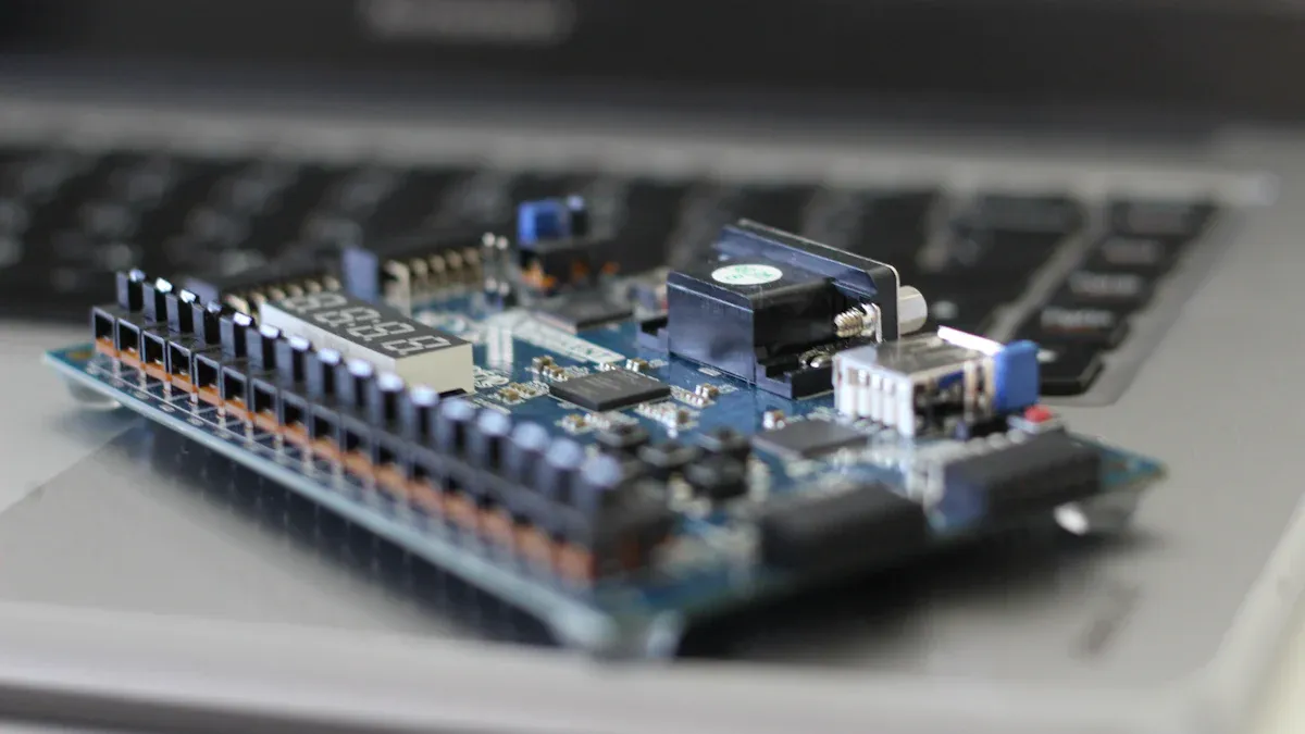
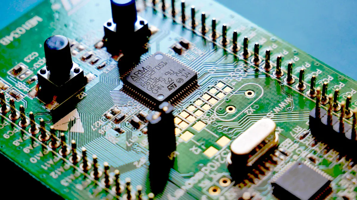


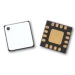
![ENC624J600-I/PT microcontroller: Datasheet, Features, Application[FAQ]](https://static.kynix.com/imgs/BlogImage-v/20230316173617653713.jpg)
![ATMEGA1280-16AU microcontroller: Datasheet, Features, Application[FAQ]](https://static.kynix.com/imgs/BlogImage-v/20230309165108141686.png)
![STM8S207CBT6 Microcontroller: Datasheet, Features, Application[FAQ]](https://static.kynix.com/imgs/BlogImage-v/20230309165213605373.png)
![2N7002P Mosfet: Datasheet, Pinout, Features [FAQ]](https://static.kynix.com/imgs/BlogImage-v/ky_bg_head_20211021173017.jpg)
![L298N Motor Driver: Datasheet, Arduino, Circuit [Video&FAQ]](https://static.kynix.com/imgs/BlogImage-v/ky_bg_head_20211021154504.jpg)
![MCP2515-I/P CAN Controller: CAD Models, Datasheet, Features [Video&FAQ]](https://static.kynix.com/imgs/BlogImage-v/ky_bg_head_20211021153456.jpg)


