The Kynix Components - Integrated Circuits (ICs)
Stay Ahead with Expert Electronics Insights,
Industry Trends, and Innovative Tips
Quick-Reference Card: AD8532 at a GlanceAttributeDetailComponent TypeDual Rail-to-Rail I/O Operational AmplifierManufacturerAnalog Devices Inc.Key Spec±250 mA High Output Drive CurrentSupply Voltage2.7V to 6V (Single-Supply)Package Options8-Lead TSSOP (ARU suffix)Lifecycle StatusActiveBest ForMultimedia audio, headphone drivers, and LCD capacitive loads1. What Is the AD8532? (Definition + Architecture)The AD8532 is a dual rail-to-rail input/output operational amplifier from Analog Devices Inc. that delivers an exceptionally high ±250 mA output drive current from a single supply. While standard op-amps typically max out around 20–30 mA, the AD8532 bridges the gap between traditional signal conditioning and low-power load driving, eliminating the need for discrete push-pull transistor stages in many designs.1.1 Core Architecture & Design PhilosophyInternally, the AD8532 is designed to be a "heavy lifter" in the analog domain. Analog Devices engineered the output stage to source and sink a quarter of an amp without phase reversal, while maintaining a relatively low quiescent current of 750 μA per amplifier. This means it can drive resistive loads (like 32-ohm headphones) or heavy capacitive loads (like LCD bias lines) directly. The unity-gain stability ensures that even when configured as a simple voltage buffer, it won't break into oscillation.1.2 Where It Fits in the Signal Chain / Power PathIn a typical system, the AD8532 sits at the very end of the signal chain. It usually takes a weak analog signal—such as the output of an audio DAC, an ASIC, or a microcontroller—and provides the necessary current buffering to drive a physical load. It acts as the muscular intermediary between delicate digital-to-analog conversion and the real world.2. Electrical Characteristics: The Numbers That Matter2.1 Power Supply & Consumption ProfileThe AD8532 operates on a strict single-supply range of 2.7V to 6V. At 750 μA per amplifier, the quiescent current is reasonable for line-powered applications, but might be slightly heavy for ultra-low-power coin-cell IoT devices. Why it matters: The 2.7V minimum allows it to run effectively off a depleted 3.3V rail or standard Li-Po battery, making it highly versatile for portable multimedia devices.2.2 Performance Specs (Speed, Accuracy, or Efficiency)With a 3 MHz bandwidth and a 5 V/μs slew rate, this op-amp is perfectly tailored for audio frequencies and standard control signals. Why it matters: 5 V/μs is fast enough to handle full-swing 20 kHz audio signals without slew-induced distortion, ensuring clean headphone driver performance.2.3 Absolute Maximum Ratings — What Will Kill ItThe absolute maximum supply voltage is 7V. Why it matters: This is a hard limit. Unlike older industrial op-amps that happily accept ±15V, accidentally connecting the AD8532 to a 12V rail or experiencing a 9V inductive spike will instantly destroy the silicon. Always clamp your supply lines.3. Pinout & Package Guide3.1 Pin-by-Pin Functional GroupsThe AD8532 utilizes the industry-standard dual op-amp pinout, making it highly compatible with existing layouts.Pin GroupPinsFunctionPowerV+ (8), V- (4)Supply rails (V- is typically grounded in single-supply)Signal InputIN1+ (3), IN1- (2), IN2+ (5), IN2- (6)Non-inverting and inverting inputs for channels 1 and 2Signal OutputOUT1 (1), OUT2 (7)High-current outputs (±250 mA capability)(Note: Refer to the official AD8532 datasheet for exact pin numbering based on your specific package variant.)3.2 Package Variants & Soldering NotesPackagePitchThermal Pad?Soldering Method8-Lead TSSOP (ARU)0.65 mmNoStandard Reflow / Hand-solderable with flux8-Lead SOIC1.27 mmNoEasy hand-soldering / Standard ReflowSoldering Note: Because this part handles high currents, ensure the PCB traces connected to the output and supply pins are wide enough to handle 250mA continuously without dangerous temperature rises.3.3 Part Number DecoderWhen ordering, pay attention to the suffixes:* AD8532: Base part number* A: Temperature/Performance grade* R: SOIC package / RU: TSSOP package* Z: RoHS Compliant (Lead-Free)* -REEL7: Tape and reel packaging (7-inch)4. Known Issues, Errata & Real-World Pain PointsWhy this section exists: Community forums, application notes, and field reports reveal problems the datasheet glosses over. This section saves you hours of debugging.Problem: Strict Voltage Limitation DamageRoot Cause: The absolute maximum supply voltage is 7V. Engineers migrating from older LM358 designs (which handle up to 32V) frequently fry the AD8532 by applying 9V or 12V.Recommended Fix: Ensure the supply voltage is strictly regulated via an LDO within the 2.7V to 6V range. Implement TVS diodes if there is any risk of voltage transients.Problem: EMI/RF SusceptibilityRoot Cause: The internal input stages can suffer from RF rectification in the few hundred MHz region, especially in low-impedance inverting architectures. This manifests as unexplained DC offsets.Recommended Fix: Add RF decoupling capacitors close to the pins, place ferrite beads on the input lines, and ensure proper ground plane shielding.Problem: Thermal Drift Under Heavy LoadRoot Cause: Sourcing/sinking 250mA generates significant localized heat within the small TSSOP package. As the die warms up, offset voltage and performance can drift, particularly in continuous audio applications.Recommended Fix: Do not treat this like a standard logic IC. Use generous PCB copper pouring around the V+ and V- pins to act as a heatsink, and avoid continuous maximum-current DC loads where possible.5. Application Circuits & Integration Examples5.1 Typical Application: Headphone DriverBecause of its 250mA drive and rail-to-rail output, the AD8532 is an excellent drop-in headphone amplifier. In this configuration, the op-amp is set up as a non-inverting amplifier with a gain of 2 or 3. A large coupling capacitor (e.g., 220μF) is placed in series with the output to block DC from reaching the headphone coils, while a 10k potentiometer at the input acts as a volume control. 5.2 Interface Example: Driving from a 3.3V Microcontroller DACWhile the AD8532 is purely analog, it is frequently paired with microcontrollers (like STM32 or ESP32) to buffer weak internal DACs. // Pseudocode for MCU DAC initialization driving an AD8532 Buffervoid init_audio_output() { // Initialize MCU DAC (0 to 3.3V range) DAC_Init(CHANNEL_1); // The AD8532 is wired as a unity-gain buffer (OUT connected to IN-) // It will mirror the DAC voltage but provide up to 250mA of current // Output a mid-rail bias voltage (1.65V) to prevent speaker popping DAC_SetValue(CHANNEL_1, 2048); // 12-bit DAC mid-scale}6. Alternatives, Replacements & Cross-Reference6.1 Pin-Compatible Drop-In ReplacementsIf you are facing allocation issues, consider these alternatives, keeping in mind their current limits.Part NumberManufacturerKey DifferenceCompatible?OPA2343Texas InstrumentsFaster (5.5MHz), lower drive current?? (Check load current)TLC2272Texas InstrumentsMuch lower noise, lower output drive?? (Check load current)TS272STMicroelectronicsHigher max voltage (16V), standard output? (Not high current)LM358Texas InstrumentsIndustry standard, NOT rail-to-rail? (Different specs)6.2 Upgrade Path (Better Performance)If you need similar high-current drive but better precision and lower noise for high-fidelity audio, consider the Texas Instruments OPA1688. It can drive heavy capacitive loads and offers superior THD+N metrics, though at a higher cost.6.3 Cost-Down AlternativesFor procurement teams looking to cut costs where the massive 250mA drive is not actually utilized by the circuit, the ON Semiconductor NCS20072 is a highly economical rail-to-rail op-amp that fits the same footprint.7. Procurement & Supply Chain IntelligenceLifecycle Status: Active. The AD8532 is a mature, widely used component with no current EOL (End of Life) warnings.Typical MOQ & Lead Time: Usually available in cut-tape for prototyping (MOQ 1) or 2,500-piece reels for production. Lead times are generally stable at 8–12 weeks, though stock is frequently held by major distributors.BOM Risk Factors: Medium. While the footprint is standard, the combination of single-supply 6V max and 250mA drive is somewhat unique. If the AD8532 goes out of stock, finding a drop-in replacement that can handle the same load current without layout changes is difficult.Recommended Safety Stock: Maintain 3–6 months of safety stock if your design relies strictly on the 250mA output capability.Authorized Distributors: Digikey, Mouser, Arrow, and Rochester Electronics.8. Frequently Asked QuestionsQ: What is the AD8532 used for?The AD8532 is primarily used for multimedia audio ports, headphone drivers, LCD bias drivers, and buffering ASIC inputs/outputs due to its high current capacity.Q: What are the best alternatives to the AD8532?Top alternatives include the Texas Instruments OPA2343 and TLC2272, though you must verify that your application does not require the AD8532's full 250mA drive, as these alternatives supply less current.Q: Is the AD8532 still in production?Yes, the AD8532 is in active production by Analog Devices and is considered a staple component in many mature designs.Q: Can the AD8532 work with 3.3V logic?Yes. Its supply range is 2.7V to 6V, making it perfectly suited for 3.3V and 5V single-supply systems. Q: Where can I find the AD8532 datasheet and evaluation board?The official datasheet and SPICE models can be downloaded directly from the Analog Devices website or via authorized distributors.9. Resources & ToolsReference Designs: Analog Devices provides extensive application notes on driving capacitive loads and headphone amplifiers.SPICE / LTspice Model: Highly recommended to simulate thermal dissipation and load driving. Available directly within LTspice or from the Analog Devices website.PCB Footprints: Standard 8-Lead TSSOP and SOIC footprints are available in SnapEDA, UltraLibrarian, and built into KiCad/Altium standard libraries.
Kynix On 2026-04-25
Quick-Reference Card: TLE7185 at a GlanceAttributeDetailComponent TypeAutomotive 3-Phase Bridge Driver ICManufacturerInfineon TechnologiesKey SpecUp to 5A Drive CapabilitySupply Voltage5.5V to 32VPackage OptionsPG-DSO-36 (with Exposed Pad)Lifecycle StatusActive (AEC-Q100 Qualified)Best ForAutomotive cooling fans, water/oil pumps, and EPS1. What Is the TLE7185? (Definition + Architecture)The TLE7185 is an automotive-grade 3-phase bridge driver IC from Infineon Technologies that controls 6 to 12 external N-channel MOSFETs to form a high-current converter for motor drives. Unlike simple gate drivers, this IC integrates an advanced charge pump, adjustable dead time, and comprehensive analog protection schemes, removing the burden of complex power-stage management from the host microcontroller.1.1 Core Architecture & Design PhilosophyAt its core, the TLE7185 is designed for harsh automotive environments where battery voltages fluctuate wildly and thermal constraints are tight. Infineon's inclusion of an integrated charge pump is the standout architectural decision here. It guarantees that the high-side external N-channel MOSFETs receive adequate gate drive voltage even if the main battery rail drops as low as 5.5V. Furthermore, the analog adjustable Short Circuit Protection (SCP) allows engineers to tune current limits without relying on digital latency, ensuring instantaneous hardware-level protection.1.2 Where It Fits in the Signal Chain / Power PathThe TLE7185 sits directly between your low-voltage logic controller (like an STM32 or automotive MCU) and the high-power 3-phase inverter bridge. It takes standard logic-level PWM signals from the MCU and translates them into high-current (up to 5A) gate drive pulses to rapidly switch the external MOSFETs, while simultaneously feeding diagnostic and fault data back upstream to the MCU.2. Electrical Characteristics: The Numbers That Matter2.1 Power Supply & Consumption ProfileSupply Voltage Range (5.5V to 32V): The wide input range is specifically tailored for 12V and 24V automotive nets. Why it matters: The 5.5V minimum threshold ensures that safety-critical motors (like power steering or fuel pumps) continue running during severe cold-cranking events when battery voltage sags significantly.Integrated Charge Pump Operation: Why it matters: This eliminates the need for external boost circuitry to drive the high-side N-channel MOSFETs, saving BOM cost and PCB real estate.2.2 Performance Specs (Speed, Accuracy, or Efficiency)Gate Drive Capability (Up to 5A): Why it matters: A 5A peak drive current allows the TLE7185 to rapidly charge and discharge the massive gate capacitances of parallel power MOSFETs, minimizing switching losses in high-current applications.6 Separate Control Inputs: Why it matters: Instead of relying on internal commutation logic, exposing all 6 channel inputs gives the firmware engineer absolute control over complex motor control algorithms like Field Oriented Control (FOC).2.3 Absolute Maximum Ratings — What Will Kill ItMaximum Operating Temperature (150°C): Why it matters: Exceeding this junction temperature will trigger the over-temperature lockout. In enclosed automotive pumps, ambient temperatures can easily exceed 105°C, leaving a narrow thermal budget for the IC's own power dissipation.Over-voltage Transients: While rated to 32V continuous, automotive load dumps can spike much higher. Why it matters: You must implement external TVS diodes to clamp load dump transients before they reach the TLE7185's supply pins.3. Pinout & Package Guide3.1 Pin-by-Pin Functional GroupsPin GroupPinsFunctionPowerVS, GNDMain supply voltage and system groundGate DriveGHx, GLx, SHxHigh-side/Low-side gate outputs and source connectionsControlIHx, ILxLogic-level PWM inputs from microcontrollerProtectionSCD, ERRShort circuit delay config and error flag outputCharge PumpCP1, CP2, VCPExternal capacitor connections for the charge pump3.2 Package Variants & Soldering NotesPackagePitchThermal Pad?Soldering MethodPG-DSO-360.65mmYes (Exposed)Reflow only (Thermal vias required)Soldering Note: Hand-soldering the PG-DSO-36 package during prototyping is notoriously difficult due to the massive exposed thermal pad underneath. A hot air rework station or reflow oven is mandatory to ensure the pad bonds completely to the PCB ground plane.3.3 Part Number DecoderTLE: Infineon Automotive IC prefix.7185: Base part number for the 3-phase bridge driver.-1E: Indicates specific silicon revision and package type (DSO with exposed pad).4. Known Issues, Errata & Real-World Pain PointsWhy this section exists: Community forums, application notes, and field reports reveal problems the datasheet glosses over. This section saves you hours of debugging.Problem: Thermal Management / Over-Temperature Lockout - Root Cause: High-current switching at high PWM frequencies generates significant internal heat. If the IC relies solely on the plastic package for heat dissipation, junction temperatures spike, triggering the internal over-temperature warning or lockout. - Recommended Fix: Ensure the exposed pad on the PG-DSO-36 package is properly soldered to a large, unbroken PCB ground plane. You must use an array of thermal vias directly under the pad to wick heat into the inner copper layers.Problem: Shoot-Through Vulnerability (Cross-Conduction) - Root Cause: Incorrectly configured dead time allows both the high-side and low-side MOSFETs on a single half-bridge to be conductive simultaneously, creating a dead short across the power rails. - Recommended Fix: Carefully calculate and set the adjustable dead time using the dedicated external resistor. Ensure the dead time exceeds the worst-case turn-off delay of your chosen MOSFETs, factoring in gate resistor values and operating temperature.5. Application Circuits & Integration Examples5.1 Typical Application: Automotive Cooling FanIn a high-power automotive HVAC or engine cooling fan, the TLE7185 is paired with six heavy-duty N-channel MOSFETs (e.g., OptiMOS? series). The IC is powered directly from the KL30 (battery) rail. A high-frequency decoupling capacitor is placed as close to the VS pin as possible. The external charge pump capacitors (typically ceramic X7R) are routed with minimal trace inductance to ensure stable high-side gate drive.5.2 Interface Example: Connecting to a MicrocontrollerThe TLE7185 requires 6 standard PWM signals from a microcontroller (like an STM32 or Aurix) configured for complementary output with dead-time insertion (though the IC provides hardware dead-time as a backup).// Pseudocode for STM32 Timer initialization driving the TLE7185void init_motor_pwm(void) { // Configure Timer 1 for 3-phase center-aligned PWM TIM1->CR1 |= TIM_CR1_CMS_1; // Center-aligned mode // Enable complementary outputs for High and Low sides (IHx, ILx) TIM1->CCER |= TIM_CCER_CC1E | TIM_CCER_CC1NE; TIM1->CCER |= TIM_CCER_CC2E | TIM_CCER_CC2NE; TIM1->CCER |= TIM_CCER_CC3E | TIM_CCER_CC3NE; // Note: Hardware dead-time on TLE7185 acts as safety net. // Set MCU dead-time slightly higher than TLE7185 resistor setting. set_mcu_deadtime(2000); // 2 microseconds}6. Alternatives, Replacements & Cross-Reference6.1 Pin-Compatible Drop-In ReplacementsCurrently, there are no exact 1:1 pin-compatible drop-in replacements from other manufacturers due to Infineon's proprietary pinout and analog protection schemes. Redesigning the PCB is required if moving away from the Infineon ecosystem.6.2 Upgrade Path (Better Performance)Part NumberManufacturerKey DifferenceCompatible?TLE7189InfineonAdvanced diagnostics, higher safety integration?? (Requires minor layout/BOM updates)Why upgrade? The TLE7189 is the logical next step for engineers designing ASIL-rated automotive systems, offering enhanced diagnostic feedback and operational amplifiers for phase current sensing.6.3 Cost-Down AlternativesIf you are designing a non-automotive system or have flexibility in your layout, consider the STMicroelectronics L6376D or the NXP MC33PF8100EQES. These provide similar 3-phase bridge driving capabilities but will require completely different schematic routing and firmware initialization.7. Procurement & Supply Chain IntelligenceLifecycle Status: Active. As an AEC-Q100 qualified part, the TLE7185 is supported by Infineon's automotive longevity program.Typical MOQ & Lead Time: Standard factory lead times fluctuate between 16 to 26 weeks. MOQs typically match full reel quantities (usually 1,000 pieces).BOM Risk Factors: Single-source risk. Because there is no exact pin-compatible alternative from competitors, a supply disruption at Infineon directly halts production.Recommended Safety Stock: Maintain a minimum of 6 months of safety stock for automotive production lines to buffer against semiconductor allocation shifts.Authorized Distributors: Mouser, Digi-Key, Avnet, and Arrow Electronics. Avoid grey-market brokers for automotive safety ICs due to counterfeit risks.8. Frequently Asked QuestionsQ: What is the TLE7185 used for? The TLE7185 is used to drive high-current 3-phase motors in automotive applications such as cooling fans, water/oil/fuel pumps, and electro-hydraulic power steering (EHPS) systems.Q: What are the best alternatives to the TLE7185? The Infineon TLE7189 is the best direct upgrade within the same family. For alternatives from other manufacturers, the STMicroelectronics L6376D and NXP MC33PF8100EQES are comparable 3-phase bridge drivers, though not pin-compatible.Q: Is the TLE7185 still in production? Yes, the TLE7185 is an Active, AEC-Q100 qualified component with long-term automotive manufacturing support from Infineon.Q: Can the TLE7185 operate during an automotive cold crank? Yes. The integrated charge pump allows the TLE7185 to maintain full gate drive capability even when the battery supply voltage drops as low as 5.5V.Q: Where can I find the TLE7185 datasheet and evaluation board? The official datasheet and corresponding evaluation kits can be downloaded and purchased directly from Infineon's website or through authorized distributors like Mouser and Digi-Key.9. Resources & ToolsEvaluation / Development Kit: Infineon BLDC Motor Control Shield with TLE718x series.Reference Designs: Infineon Application Notes on "Automotive 3-Phase Motor Control" and "Thermal Management for DSO Packages".Community Libraries: STM32CubeMX motor control workbench (requires manual configuration for TLE7185 hardware limits).SPICE / LTspice Model: Transient thermal and electrical models are available via the Infineon Developer Center.
Kynix On 2026-04-25
Quick-Reference Card: AD7845 at a GlanceAttributeDetailComponent Type12-Bit Multiplying Digital-to-Analog Converter (MDAC)ManufacturerAnalog Devices Inc.Key Spec4-Quadrant Multiplication with On-Chip AmplifierSupply Voltage±12 V to ±15 V Dual SupplyPackage OptionsDIP, PLCC, SOIC (Refer to datasheet for exact suffixes)Lifecycle StatusObsolete / NRND (Critical procurement risk)Best ForAutomatic Test Equipment (ATE) & Programmable Power Supplies1. What Is the AD7845? (Definition + Architecture)The AD7845 is a 12-bit multiplying digital-to-analog converter (MDAC) from Analog Devices Inc. that integrates an on-chip output amplifier to deliver complete 4-quadrant multiplication. For hardware engineers, the integration of the output amplifier is the defining feature; it eliminates the need for an external precision op-amp, removing a major source of parasitic capacitance, offset errors, and BOM bloat that plagued earlier MDAC designs.1.1 Core Architecture & Design PhilosophyFabricated on Analog Devices' proprietary LC2MOS process, the AD7845 combines precision bipolar analog circuitry with low-power CMOS logic. Internally, it utilizes an inverted R-2R ladder network. What makes this architecture highly reliable is the inclusion of matched application resistors directly on the silicon. Because these resistors share the same thermal gradient and manufacturing tolerances as the R-2R ladder, they guarantee monotonic performance across the entire operating temperature range.1.2 Where It Fits in the Signal Chain / Power PathThe AD7845 sits directly between your digital control logic (MCU, DSP, or FPGA) and your high-voltage analog output stage. It is typically driven by a parallel digital bus and a precision bipolar reference voltage. Downstream, its ±10V capable output directly drives actuators, programmable attenuators, or the control loops of programmable power supplies.2. Electrical Characteristics: The Numbers That Matter2.1 Power Supply & Consumption ProfileThe AD7845 requires a dual bipolar power supply, specifically ±12 V to ±15 V. Why it matters: Modern digital systems are heavily 3.3V or 5V single-supply. Designing in the AD7845 requires a dedicated bipolar switching regulator or charge pump if your system lacks legacy analog rails. Despite the high-voltage analog rails, the digital inputs are fully TTL and 5V CMOS compatible, saving you from needing external level shifters.2.2 Performance Specs (Speed, Accuracy, or Efficiency)Resolution: 12-Bit. Provides 4096 distinct output steps, standard for industrial control.Settling Time: 2.5 μs. Why it matters: In Automatic Test Equipment (ATE), settling time dictates your test throughput. A 2.5 μs settling time is fast enough for low-to-medium frequency waveform generation but will bottleneck high-speed RF testing.Total Harmonic Distortion (THD): -90 dB typ. Ensures clean signal reproduction when used as a digital audio attenuator or in precision waveform synthesis.Minimum Load Resistance: 2 kΩ. Do not attempt to drive low-impedance loads (like 50Ω RF lines or speakers) directly without an external buffer.2.3 Absolute Maximum Ratings — What Will Kill ItVDD to VSS Reversal: Reversing the bipolar supply rails will cause immediate catastrophic latch-up.Digital Input Overvoltage: Applying logic signals higher than VDD + 0.3V or lower than GND - 0.3V will forward-bias the internal ESD diodes, potentially destroying the CMOS input stage. Always ensure the analog rails are powered up before applying digital signals.3. Pinout & Package Guide3.1 Pin-by-Pin Functional GroupsPin GroupPinsFunctionPowerVDD, VSS, GNDDual supply rails (±12V to ±15V) and system ground.Digital InputsDB0 to DB1112-bit parallel data bus. DB11 is the MSB.Control/CS, /WRChip Select and Write logic for latching data into the DAC register.AnalogVREF, VOUTReference voltage input and buffered analog voltage output.FeedbackRFB, ROFSInternal matched resistors for gain ranging and bipolar offset.3.2 Package Variants & Soldering NotesPackagePitchThermal Pad?Soldering MethodDIP (Plastic/Ceramic)2.54 mmNoWave solder or hand solderPLCC1.27 mmNoReflow or socketedSOIC1.27 mmNoStandard IR ReflowNote: As a legacy component, the AD7845 is often found in through-hole DIP packages, making it excellent for prototyping but bulky for modern PCB layouts.3.3 Part Number DecoderAD: Analog Devices standard prefix.7845: Base part number.A/B/C/S: Indicates linearity grade and temperature range (e.g., Commercial, Industrial, Military). Refer to the datasheet for exact LSB error tolerances per grade.N/R/P: Package designator (N = PDIP, R = SOIC, P = PLCC).4. Known Issues, Errata & Real-World Pain PointsWhy this section exists: Community forums, application notes, and field reports reveal problems the datasheet glosses over. This section saves you hours of debugging.Problem 1: Ground Noise Susceptibility * Root Cause: High-frequency noise on the input common can couple directly to the output via the internal compensation capacitor. Furthermore, common impedance in the negative supply line (VSS) can cause severe interference and degrade the -90 dB THD. * Recommended Fix: Use a subtractor circuit for the analog input. Ensure the internal amplifier is powered with respect to the output signal common to maximize common-mode rejection. Implement strict star-grounding techniques separating analog and digital return paths.Problem 2: Obsolescence and Availability * Root Cause: The LC2MOS process is heavily outdated. The AD7845 is marked as obsolete or "Not Recommended for New Designs" (NRND) across major distributors. * Recommended Fix: Do not design this into new boards. For existing product maintenance, procure remaining stock through authorized legacy distributors like Rochester Electronics. For redesigns, migrate to newer SPI/I2C precision DACs (e.g., AD57xx series).5. Application Circuits & Integration Examples5.1 Typical Application: 4-Quadrant Multiplying DACIn a 4-quadrant configuration, the AD7845 can accept both positive and negative reference voltages, and output both positive and negative voltages based on the digital code. This is heavily used in programmable power supplies to digitally scale an AC reference signal. By utilizing the internal RFB and ROFS resistors, you eliminate the need for external precision resistor networks to shift the unipolar DAC output into a bipolar range.5.2 Interface Example: Connecting to a MicrocontrollerBecause the AD7845 uses a legacy parallel interface, driving it requires 12 GPIO pins for data, plus 2 for control (/CS and /WR). Here is the initialization and write sequence for an STM32 or Arduino:// Pseudocode for AD7845 Parallel Writevoid write_AD7845(uint16_t dac_value) { // 1. Ensure /CS and /WR are HIGH (idle state) digitalWrite(CS_PIN, HIGH); digitalWrite(WR_PIN, HIGH); // 2. Place 12-bit value on the parallel bus (DB0-DB11) set_gpio_bus(dac_value & 0x0FFF); // 3. Pull /CS LOW to select chip digitalWrite(CS_PIN, LOW); // 4. Pulse /WR LOW then HIGH to latch data digitalWrite(WR_PIN, LOW); delayMicroseconds(1); // Satisfy minimum write pulse width digitalWrite(WR_PIN, HIGH); // 5. Release /CS digitalWrite(CS_PIN, HIGH);}6. Alternatives, Replacements & Cross-ReferenceIf you are facing supply chain blocks or redesigning an older board, consider these alternatives.6.1 Pin-Compatible Drop-In ReplacementsPart NumberManufacturerKey DifferenceCompatible?MX7845Maxim IntegratedVirtually identical specs and pinout? YesSP7545SipexSimilar architecture, verify settling time?? Check Specs6.2 Upgrade Path (Better Performance)If redesigning the PCB, abandon the parallel interface and ±15V logic. Move to modern SPI/I2C DACs like the Analog Devices AD5722 (dual 12-bit, software-programmable bipolar output) which saves massive board space and reduces power supply complexity.6.3 Cost-Down AlternativesLegacy parts like the Burr-Brown (TI) DAC667 or Maxim MAX528 were historic competitors. However, finding cheap stock of any of these legacy parallel DACs is difficult today. True cost-down requires migrating to modern serial DACs.7. Procurement & Supply Chain IntelligenceLifecycle Status: Obsolete / NRND. Analog Devices has largely phased out this component.Typical MOQ & Lead Time: Factory lead times are no longer applicable. Stock is limited to what is currently on distributor shelves.BOM Risk Factors: Extreme risk. Single-source reliance on a discontinued part will halt production lines.Recommended Safety Stock: Buy out available inventory from authorized legacy suppliers if your product cannot be redesigned.Authorized Distributors: Rochester Electronics is the primary authorized source for end-of-life (EOL) Analog Devices silicon. Avoid grey-market brokers to prevent counterfeit ICs.8. Frequently Asked QuestionsQ: What is the AD7845 used for? The AD7845 is primarily used in Automatic Test Equipment (ATE), programmable power supplies, digital attenuators, and digital-to-4–20 mA converters. Its integrated amplifier makes it ideal for precision analog scaling.Q: What are the best alternatives to the AD7845? The Maxim Integrated MX7845 is the closest pin-compatible drop-in replacement. Other historic competitors include the Burr-Brown DAC667 and Sipex SP7545, though availability for all is scarce.Q: Is the AD7845 still in production? No, the AD7845 is generally considered obsolete and is Not Recommended for New Designs (NRND). Buyers must rely on legacy distributors for remaining stock.Q: Can the AD7845 work with 3.3V logic? The AD7845 digital inputs are TTL and 5V CMOS compatible. While some 3.3V logic high levels may meet the minimum VIH requirements, you must verify against the datasheet to ensure reliable triggering across temperature variations.Q: Where can I find the AD7845 datasheet and schematic symbols? Datasheets, CAD models, and legacy application notes can be found on the Analog Devices Inc. website or through authorized legacy distributors like Rochester Electronics.9. Resources & ToolsEvaluation / Development Kit: No longer actively manufactured; rely on legacy stock or build a custom breakout board.Reference Designs: Search the Analog Devices archive for legacy application notes on "LC2MOS MDAC Applications".Community Libraries: Parallel DACs generally do not require complex libraries; simple GPIO bit-banging (as shown in Section 5) is sufficient for Arduino/STM32 integration.SPICE / LTspice Model: Check the Analog Devices LTspice library for legacy macro models, though exact transient models for the internal op-amp may be limited.
Kynix On 2026-04-24
Quick-Reference Card: HEXFET at a GlanceAttributeDetailComponent TypeN-Channel Power MOSFETManufacturerInfineon TechnologiesKey Spec13.9 mΩ Rds(on) @ 10VSupply Voltage55V Vdss (Maximum)Package OptionsThrough Hole TO-262 (I2PAK)Lifecycle StatusObsolete (Legacy IRFZ44ZL variants)Best ForBattery Operated Drives & DC-DC Converters1. What Is the HEXFET? (Definition + Architecture)The HEXFET is a N-channel power MOSFET from Infineon Technologies that provides fast switching and ultra-low on-resistance for rugged power applications. Originally developed by International Rectifier (now part of Infineon), the HEXFET architecture revolutionized power switching by utilizing a hexagonal cell structure to maximize silicon density and minimize conduction losses.1.1 Core Architecture & Design PhilosophyAt its core, this specific HEXFET generation utilizes an advanced trench process technology. The manufacturer prioritized achieving the lowest possible Rds(on) (13.9 mΩ) per silicon area while maintaining a fully avalanche-rated structure. This means the die can safely absorb energy transients during inductive load switching without catastrophic failure, a critical feature for motor drives and energy harvesting systems.1.2 Where It Fits in the Signal Chain / Power PathThis component sits at the very end of your control chain as the primary power switch. It is driven downstream by a dedicated gate driver IC or controller and sits upstream of high-current inductive loads (like motors or transformers) or resistive loads.2. Electrical Characteristics: The Numbers That Matter2.1 Power Supply & Consumption ProfileThe drain-to-source breakdown voltage (Vdss) is rated at 55V, giving you comfortable headroom for 12V, 24V, and 36V bus systems. However, the most critical number for your control circuitry is the Gate Charge (Qg) of 43 nC @ 10V. This is not a logic-level MOSFET; it requires a stiff 10V gate drive to fully enhance the channel. Trying to drive this directly from a 3.3V microcontroller will leave the FET in its linear region, leading to massive thermal dissipation and immediate failure.2.2 Performance Specs (Speed, Accuracy, or Efficiency)The standout performance metric is the 13.9 mΩ Rds(on) combined with a continuous drain current (Id) of 51A. For the designer, this translates to extremely low conduction losses ($I^2R$). At a continuous 20A load, the FET will only dissipate about 5.5W of heat, making it highly efficient for DC-DC converters and isolated primary-side switching.2.3 Absolute Maximum Ratings — What Will Kill ItMaximum Power Dissipation (80W): Do not treat this as a continuous operating target. Dissipating 80W requires aggressive active cooling and a massive heatsink.Drain-to-Source Voltage (55V): Exceeding this limit, even during microsecond inductive voltage spikes, will push the device into avalanche breakdown.Continuous Drain Current (51A): This is a package-limited and thermally-limited absolute maximum.3. Pinout & Package Guide3.1 Pin-by-Pin Functional GroupsPin GroupPinsFunctionControlGate (1)High-impedance voltage control input. Requires 10V to fully enhance.Power InDrain (2, Tab)Connected to the load in low-side switching topologies.Power OutSource (3)Typically connected to system ground in N-channel applications.3.2 Package Variants & Soldering NotesPackagePitchThermal Pad?Soldering MethodTO-262 (I2PAK)2.54mmYes (Exposed Tab)Through-hole wave soldering or manual hand-solderThe TO-262 package is essentially a D2PAK without the bent surface-mount leads. The large metal tab is electrically connected to the Drain. If mounting to a grounded chassis, you must use a thermal insulator pad (like Sil-Pad) and an insulating shoulder washer to prevent a dead short.3.3 Part Number DecoderUsing the legacy IRFZ44ZL as an example: - IRF: International Rectifier (Infineon) standard MOSFET prefix. - Z: Trench technology / Generation identifier. - 44: Current/Voltage capability class indicator. - Z: Specific die revision. - L: TO-262 (I2PAK) package designation.4. Known Issues, Errata & Real-World Pain PointsWhy this section exists: Community forums, application notes, and field reports reveal problems the datasheet glosses over. This section saves you hours of debugging.Problem: Component Obsolescence - Root Cause: Specific legacy variants like the IRFZ44ZL are marked as obsolete as manufacturing shifts to newer, higher-density silicon processes. - Recommended Fix: Transition immediately to active parametric equivalents like the IRFZ44ZLPBF (RoHS compliant), IRFZ48NSTRLPBF, or migrate to Infineon's newer OptiMOS series.Problem: Microcontrollers Failing to Switch the Load - Root Cause: The gate requires a 10V gate-to-source voltage (Vgs) to achieve the ultra-low 13.9 mΩ Rds(on). It is unsuitable for direct 3.3V or 5V logic drive. - Recommended Fix: Insert a dedicated gate driver IC (e.g., TC4420) between the MCU and the MOSFET, or redesign the BOM to use a logic-level equivalent (e.g., IRLZ44N).Problem: Thermal Runaway Under Heavy Load - Root Cause: High power dissipation (up to 80W max) at continuous high currents will rapidly exceed the $175^circ C$ junction temperature limit if relying solely on ambient air cooling. - Recommended Fix: Ensure proper thermal management by bolting the TO-262 tab to an adequate aluminum heatsink using high-quality thermal interface material.5. Application Circuits & Integration Examples5.1 Typical Application: DC-DC ConvertersIn a standard buck or boost DC-DC converter, this HEXFET operates as the primary high-speed switch. Because it is an N-channel device, it is easiest to implement as a low-side switch. The source is tied to ground, and the drain is connected to the inductor or transformer primary. A gate resistor (typically 10Ω to 47Ω) is placed in series with the gate to dampen parasitic ringing caused by the gate capacitance and trace inductance.5.2 Interface Example: Connecting to a MicrocontrollerBecause this HEXFET requires a 10V gate drive, you cannot connect it directly to an STM32 or ESP32 GPIO. You must use a gate driver IC powered by a 12V rail.// Pseudocode for driving a gate driver IC connected to the HEXFET#define PWM_PIN 9#define PWM_FREQ 20000 // 20 kHz switching frequencyvoid init_HEXFET_Control() { // Configure MCU pin for PWM output to the Gate Driver IC setup_pwm(PWM_PIN, PWM_FREQ); // Start with 0% duty cycle (HEXFET OFF) set_pwm_duty_cycle(PWM_PIN, 0); }void ramp_up_motor() { // Gradually increase duty cycle to safely spin up a DC motor for(int duty = 0; duty <= 100; duty++) { set_pwm_duty_cycle(PWM_PIN, duty); delay_ms(10); }}6. Alternatives, Replacements & Cross-Reference6.1 Pin-Compatible Drop-In ReplacementsIf you are facing allocation issues with the IRFZ44ZL, these parts offer similar specs in the same or compatible packages.Part NumberManufacturerKey DifferenceCompatible?IRFZ44ZLPBFInfineonLead-free (RoHS) version of the exact part?IRFZ48ZInfineonSlightly higher current rating?IRF3205LInfineonMuch higher current (110A), higher gate charge??STP50N06STMicroelectronics60V, 50A, slightly higher Rds(on)?6.2 Upgrade Path (Better Performance)If redesigning the board, look at Infineon's OptiMOS line. You can achieve the same 55V/50A ratings in much smaller, surface-mount packages (like SuperSO8 or DFN) with significantly lower gate charge, allowing for faster switching frequencies and smaller passive components.6.3 Cost-Down AlternativesFor high-volume procurement, second-source legacy parts from manufacturers like STMicroelectronics (e.g., STP50N06) or Vishay often provide excellent cost-down opportunities for general-purpose power switching where absolute cutting-edge Rds(on) is not strictly required.7. Procurement & Supply Chain IntelligenceLifecycle Status: The specific legacy IRFZ44ZL is Obsolete. Procurement teams must update BOMs to the PbF (Lead-Free) suffix or cross-reference to active alternatives.Typical MOQ & Lead Time: For active equivalents, standard MOQs are typically 1,000 units (tube/tape and reel) with lead times hovering around 12–16 weeks depending on silicon availability.BOM Risk Factors: High risk if the exact obsolete part number is hard-coded into the AVL (Approved Vendor List). Ensure engineering approves the STP50N06 or IRF3205L as alternate sources.Recommended Safety Stock: Maintain 3-6 months of safety stock for power MOSFETs due to their susceptibility to automotive supply chain fluctuations.Authorized Distributors: Always source through authorized channels (Digi-Key, Mouser, Avnet, Arrow) to avoid counterfeit power FETs, which often fail catastrophically under load.8. Frequently Asked QuestionsQ: What is the HEXFET used for? The HEXFET is primarily used as a high-efficiency power switch in battery-operated drives, DC-DC converters, isolated primary-side topologies, and general-purpose power switching.Q: What are the best alternatives to the HEXFET? For the legacy 55V variants, excellent alternatives include the Infineon IRFZ48Z, IRF3205L, and the STMicroelectronics STP50N06.Q: Is the HEXFET still in production? While the HEXFET brand and many parts are still active, specific legacy part numbers like the IRFZ44ZL are obsolete. You must transition to newer parametric equivalents or RoHS-compliant versions.Q: Can the HEXFET work with 3.3V logic? No. This specific HEXFET requires a 10V gate-to-source voltage to achieve its rated 13.9 mΩ on-resistance. You must use a gate driver IC when interfacing with 3.3V or 5V microcontrollers.Q: Where can I find the HEXFET datasheet and evaluation board? Official datasheets, SPICE models, and application notes are available directly on the Infineon Technologies website or through major authorized electronics distributors.9. Resources & ToolsEvaluation / Development Kit: Infineon Motor Control Application Kits (EVAL_MOT_DRIVE)Reference Designs: Application notes from Infineon Technologies on DC-DC converter layoutsCommunity Libraries: PlatformIO / STM32CubeMX generic PWM generation examples for gate driversSPICE / LTspice Model: Available directly from the Infineon manufacturer product page
Kynix On 2026-04-21
Quick-Reference Card: TLE5027C at a GlanceAttributeDetailComponent TypeDifferential Speed SensorManufacturerInfineon TechnologiesKey Spec-40°C to 175°C Operating TemperatureSupply VoltageRefer to the official datasheet for exact valuesPackage OptionsPG-SSO-3 (3-Pin)Lifecycle StatusActive (Automotive AEC-Q100 Qualified)Best ForAutomatic transmission and engine speed sensing1. What Is the TLE5027C? (Definition + Architecture)The TLE5027C is an iGMR-based differential speed sensor from Infineon Technologies that provides high-accuracy powertrain speed sensing with first-pulse rotation direction detection. Unlike traditional Hall-effect sensors that rely on the Lorentz force, this sensor utilizes Giant Magneto Resistive (iGMR) technology. This fundamental shift in physics allows the sensor to detect much smaller changes in magnetic fields, translating to significantly larger allowable air-gaps and drastically reduced jitter across varying frequencies and temperatures.1.1 Core Architecture & Design PhilosophyInfineon designed the TLE5027C to solve a specific automotive challenge: acquiring reliable speed and direction data immediately upon system startup, even when mechanical tolerances are loose. The internal architecture integrates the iGMR sensing bridge, a signal conditioning ASIC, and a self-calibration algorithm into a single package. The self-calibration ensures that offset drifts caused by temperature swings or mechanical wear are compensated for dynamically, preventing skipped pulses at high rotational speeds.1.2 Where It Fits in the Signal Chain / Power PathThis component sits at the very edge of the signal chain, physically mounted near a magnetic encoder wheel or a ferromagnetic toothed gear (typically on a camshaft, crankshaft, or transmission shaft). It acts as the primary data acquisition node, converting mechanical rotation into a clean, three-wire digital PWM voltage signal that is fed directly downstream to an Engine Control Unit (ECU) or Transmission Control Unit (TCU).2. Electrical Characteristics: The Numbers That Matter2.1 Power Supply & Consumption ProfileBecause this is a 3-wire sensor (VCC, GND, OUT), the power supply must be stable to prevent false triggering in the iGMR bridge. While exact supply voltage ranges depend on the specific automotive rail it's tied to (refer to the official datasheet for exact values), designers must ensure adequate local decoupling. Supply noise directly impacts the internal ADC and signal conditioning thresholds, which can degrade the sensor's otherwise excellent jitter performance.2.2 Performance Specs (Speed, Accuracy, or Efficiency)The standout performance metric of the TLE5027C is its extreme thermal tolerance: -40°C to 175°C. This makes it suitable for direct mounting on engine blocks or inside transmission housings where standard 125°C or 150°C sensors would fail. Furthermore, the PWM output interface encodes both speed (via frequency) and rotation direction (via duty cycle or pulse width), providing critical diagnostic data to the microcontroller on the very first output pulse.2.3 Absolute Maximum Ratings — What Will Kill ItExceeding the thermal limit of 175°C for prolonged periods will permanently degrade the iGMR elements. Additionally, because it is deployed in harsh automotive environments, the sensor is susceptible to severe overvoltage transients (load dumps). If external clamping and reverse-polarity protection are not implemented on the ECU side, voltage spikes will destroy the internal ASIC.3. Pinout & Package Guide3.1 Pin-by-Pin Functional GroupsPin GroupPinsFunctionPowerVCC, GNDSupply voltage and ground referenceSignal OutputOUTThree-wire digital voltage interface (PWM) for speed/direction3.2 Package Variants & Soldering NotesPackagePitchThermal Pad?Soldering MethodPG-SSO-3Standard Through-HoleNoWave Soldering / Hand SolderingThe PG-SSO-3 (Plastic Green Single Small Outline) package is specifically designed for integration into custom over-molded sensor housings. The long leads allow for welding or soldering directly to lead frames before the entire assembly is potted in epoxy to withstand transmission fluids and engine oil.3.3 Part Number DecoderTLE: Infineon Automotive IC prefix5027: Specific iGMR differential speed sensor familyC: Indicates the specific revision or output protocol variant (PWM voltage interface)4. Known Issues, Errata & Real-World Pain PointsWhy this section exists: Community forums, application notes, and field reports reveal problems the datasheet glosses over. This section saves you hours of debugging.Problem: EMC/ESD Susceptibility in High Power Environments - Root Cause: In harsh environments like hybrid and electric vehicles (HEV/EV), high-voltage switching generates severe electromagnetic interference that can couple into the sensor wiring, causing false pulses. - Recommended Fix: Implement robust external circuit protection (TVS diodes, ferrite beads) on the ECU side, or upgrade to the newer TLE5028C which features improved internal EMC/ESD immunity.Problem: Air-Gap Variations Causing Jitter - Root Cause: While iGMR technology offers excellent air-gap performance, severe mechanical vibrations in the transmission can cause dynamic air-gap fluctuations that the internal compensation algorithm struggles to track instantly. - Recommended Fix: Ensure a rigid Twist-Independent Mounting (TIM) strategy and utilize the sensor's self-calibration algorithm to allow for fast, stable start-ups.Problem: Stray Magnetic Interference - Root Cause: High-power traction motors in EVs generate massive stray magnetic fields that can oversaturate or interfere with the highly sensitive GMR sensing elements. - Recommended Fix: Implement physical magnetic shielding around the sensor housing, or utilize dual-sensor redundant configurations for safety-critical (ASIL) applications.5. Application Circuits & Integration Examples5.1 Typical Application: Automatic Transmission SystemsIn an automatic transmission, the TLE5027C is mounted facing a ferromagnetic target wheel attached to the input or output shaft. As the gear teeth pass the sensor, the iGMR bridge detects the changing magnetic vector. A back-bias magnet is typically required in the housing assembly to provide the static magnetic field that the gear teeth modulate. The sensor outputs a PWM signal where the frequency represents shaft RPM, and the pulse width indicates forward or reverse rotation.5.2 Interface Example: Connecting to a MicrocontrollerTo read the TLE5027C, the microcontroller must measure both the frequency and the pulse width of the incoming signal. This is typically done using an advanced timer peripheral in input capture mode.// Pseudocode for STM32 / Automotive MCU Timer Input Capturevoid init_TLE5027C_Capture() { // Configure Timer for Input Capture on Rising and Falling edges HAL_TIM_IC_Start_IT(&htim2, TIM_CHANNEL_1); }void HAL_TIM_IC_CaptureCallback(TIM_HandleTypeDef *htim) { if (rising_edge) { start_time = capture_value; } else { pulse_width = capture_value - start_time; // Decode direction: e.g., 45us = Forward, 90us = Reverse direction = decode_direction(pulse_width); } // Calculate RPM based on period between consecutive rising edges}6. Alternatives, Replacements & Cross-Reference6.1 Pin-Compatible Drop-In ReplacementsWhile direct drop-in replacements for 3-pin SSO packages exist, the internal output protocols (PWM pulse widths) often differ between manufacturers, requiring software updates on the ECU.Part NumberManufacturerKey DifferenceCompatible?ATS SeriesAllegro MicroSystemsUses Hall-effect instead of iGMR?? (Software tweak needed)MLX SeriesMelexisDifferent magnetic sensitivity?? (Requires validation)HAL SeriesTDK-MicronasHall-effect based?? (Different air-gap tolerance)6.2 Upgrade Path (Better Performance)If EMC/ESD is a primary concern, the TLE5028C is the direct upgrade path. It offers the same iGMR benefits but features a hardened internal architecture designed specifically to withstand the aggressive electrical environments of modern EV powertrains.6.3 Cost-Down AlternativesFor non-critical industrial speed sensing where the 175°C automotive rating is unnecessary, standard Hall-effect sensors from NXP Semiconductors or Allegro can serve as cost-down alternatives, though they will require a tighter mechanical air-gap tolerance.7. Procurement & Supply Chain IntelligenceLifecycle Status: Active. AEC-Q100 qualified for automotive use.Typical MOQ & Lead Time: Automotive sensors typically carry higher MOQs (often full reels or tubes of 1,000+ pieces) and lead times can stretch to 26-52 weeks during automotive IC crunches.BOM Risk Factors: As a proprietary iGMR sensor, it is functionally single-source. While Allegro and Melexis make alternatives, they are not exact identical drop-ins without ECU software changes.Recommended Safety Stock: Maintain a minimum of 6 months safety stock due to the historically volatile nature of the automotive semiconductor supply chain.Authorized Distributors: Always source through authorized channels like Mouser, Digi-Key, or directly from Infineon to avoid counterfeit automotive safety components.8. Frequently Asked QuestionsQ: What is the TLE5027C used for? It is primarily used for high-accuracy automotive speed sensing, including automatic transmission systems, engine speed sensing (crankshaft/camshaft), and wheel speed sensing for ABS/ESP.Q: What are the best alternatives to the TLE5027C? The closest functional alternatives are the Allegro ATS series, Melexis MLX series, and TDK-Micronas HAL series, though they may use Hall-effect technology instead of iGMR.Q: Is the TLE5027C still in production? Yes, the TLE5027C is an active, AEC-Q100 qualified component fully supported by Infineon.Q: Can the TLE5027C work with 3.3V logic? The output is a PWM digital voltage interface, but you must refer to the datasheet Table for exact VOH/VOL levels to determine if direct 3.3V compatibility is supported without a level shifter.Q: Where can I find the TLE5027C datasheet and evaluation board? The official datasheet and compatible Speed Sensor Evaluation Kits can be found directly on the Infineon Technologies website or through major authorized distributors.9. Resources & ToolsEvaluation / Development Kit: Infineon Speed Sensor Eval Kit (Check manufacturer site for specific TLE502x board)Reference Designs: Application notes from Infineon Technologies covering Twist-Independent Mounting (TIM)Community Libraries: Automotive AUTOSAR MCAL drivers typically handle the complex timer captures required for this sensor.SPICE / LTspice Model: Magnetic simulation models (e.g., ANSYS Maxwell) are more relevant than SPICE for verifying the target wheel and back-bias magnet design.
Kynix On 2026-04-21
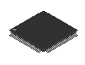
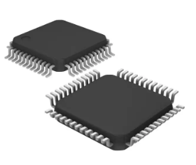
Quick-Reference Card: MPC56xx Qorivva (SPC560xB/C) at a GlanceAttributeDetailComponent Type32-bit Automotive MicrocontrollerManufacturerNXP USA Inc.Key SpecMassive connectivity: Up to 6x CAN and 10x LINFlexSupply VoltageRefer to official datasheet for exact VDD rangesPackage Options100-LQFPLifecycle StatusActive (Automotive longevity program applies)Best ForAutomotive Body Electronics & ECUs1. What Is the MPC56xx Qorivva (SPC560xB/C)? (Definition + Architecture)The MPC56xx Qorivva (SPC560xB/C) is a 32-bit automotive microcontroller from NXP USA Inc. that leverages the e200z0h Power Architecture core to manage complex in-vehicle networking and body electronics. Designed as a workhorse for automotive control units, it bridges the gap between legacy 16-bit controllers and high-end multi-core processors by offering deterministic execution and massive peripheral integration.1.1 Core Architecture & Design PhilosophyAt its heart, this MCU runs on the 32-bit e200z0h Power Architecture core clocked at 48 MHz. The design philosophy here prioritizes I/O density and reliable communication over raw compute power. It includes 384 KB of standard Flash memory alongside 64 KB of dedicated DataFlash. This DataFlash is critical: it allows designers to emulate EEPROM for storing calibration data and fault codes without needing an external memory chip on the BOM. 1.2 Where It Fits in the Signal Chain / Power PathIn a vehicle's system architecture, the MPC56xx sits at the center of a Body Control Module (BCM) or gateway node. It acts as the primary data aggregator—taking in analog signals from cabin sensors via its 10-bit/12-bit ADCs, processing the logic, and issuing commands downstream to motor drivers, relays, or smart switches. Simultaneously, it broadcasts state data upstream to the main vehicle network via its CAN or LIN buses.2. Electrical Characteristics: The Numbers That Matter2.1 Power Supply & Consumption ProfileBecause it is designed for always-on automotive environments, power management is heavily segmented. While the exact core and I/O voltages depend on the specific sub-variant (refer to the official datasheet for exact values), engineers must pay close attention to the quiescent current (Iq) in STOP and STANDBY modes. Body controllers are directly tied to the battery; poor sleep state management on this MCU will drain a vehicle's battery during long parking periods. 2.2 Performance Specs (Speed, Accuracy, or Efficiency)The 48 MHz clock speed might seem slow compared to consumer microcontrollers, but in the deterministic world of Power Architecture, it provides more than enough MIPS for real-time control loops. The integration of both 10-bit and 12-bit ADCs gives designers flexibility: use the 10-bit channels for simple voltage monitoring (like switch states) and the 12-bit channels for precise sensor measurements (like thermistors). 2.3 Absolute Maximum Ratings — What Will Kill ItThe most notable constraint in the spec sheet is the Operating Temperature range of -40°C to 85°C. Why it matters: A maximum of 85°C strictly limits this variant to in-cabin applications (doors, seats, dashboard). If you place this 85°C-rated part in an under-hood ECU or near the transmission, thermal runaway and premature silicon failure are guaranteed.3. Pinout & Package Guide3.1 Pin-by-Pin Functional GroupsPin GroupPinsFunctionPowerVDD, VSS, VDDA, VSSACore, I/O, and dedicated analog supply rails.CommunicationTX/RXUp to 6x CAN, 6x SPI, and 10x LINFlex routing.Analog InputsANxDedicated pins for the 10-bit/12-bit ADC modules.Debug/ControlJTAG/NexusProgramming, debugging, and reset (RESET_B) interfaces.3.2 Package Variants & Soldering NotesPackagePitchThermal Pad?Soldering Method100-LQFP0.5 mmNoStandard Reflow / Automated Optical Inspection (AOI) friendlyEngineering Note: The 100-LQFP (Low-profile Quad Flat Package) is highly favored in automotive manufacturing because its extended leads allow for easy visual and automated solder joint inspection, unlike QFN or BGA packages. 3.3 Part Number DecoderMPC / SPC: Denotes the Freescale/NXP Power Architecture lineage.56: Family identifier (Qorivva 32-bit).0: Core tier (e200z0).B/C: Feature set and memory tier (Body/Gateway focus).4. Known Issues, Errata & Real-World Pain PointsWhy this section exists: Community forums, application notes, and field reports reveal problems the datasheet glosses over. This section saves you hours of debugging.1. CensorShip Configuration Lockout* Problem: Engineers frequently report connection failures and an inability to download programs via the CodeWarrior IDE after configuring the MCU's "CensorShip" security feature, even when the correct password is provided.* Root Cause: Desynchronization between the IDE's debug probe timing and the MCU's secure boot sequence, or an incomplete flash configuration block.* Recommended Fix: Verify your CodeWarrior version compatibility. Ensure the hardware reset line is properly controlled by the debugger. If locked out, utilize NXP community-provided configuration scripts designed specifically for recovering CensorShip-locked devices.2. Data Flash Array Read Exceptions* Problem: Unhandled exceptions and hard faults occur when attempting to read from the 64KB DataFlash Array during runtime execution.* Root Cause: The DataFlash requires specific timing wait-states and initialization commands before it can be read, unlike standard program flash. * Recommended Fix: Carefully review your firmware initialization routines. Ensure the flash memory controller is fully initialized with the correct clock dividers and access procedures before any application code attempts to fetch data from the EEPROM emulation area.5. Application Circuits & Integration Examples5.1 Typical Application: Automotive Body Control Module (BCM)In a typical BCM, the MPC560xB acts as the central node for a vehicle door. It reads window switch states via GPIO, controls window motors via external H-bridges (driven by the MCU's 16-bit timers generating PWM), and communicates with the main dashboard ECU via CAN. The 10 LINFlex channels act as master nodes to control localized, low-speed peripherals like RGB ambient lighting or mirror adjustment motors.5.2 Interface Example: Initializing the CAN ModuleWhen bringing up the MCU bare-metal, initializing the FlexCAN module requires configuring the clock, setting the baud rate, and unfreezing the peripheral. // Pseudocode for MPC56xx FlexCAN Initializationvoid init_FlexCAN_0(void) { // 1. Enter Freeze Mode to allow configuration CAN_0.MCR.B.MDIS = 0; // Enable CAN module CAN_0.MCR.B.HALT = 1; // Request halt while(!CAN_0.MCR.B.FRZACK){} // Wait for Freeze Acknowledge // 2. Configure Baud Rate (e.g., 500 kbps based on 48MHz clock) CAN_0.CR.R = 0x04DB0006; // Set Prescaler, PSEG1, PSEG2, PROPSEG // 3. Exit Freeze Mode CAN_0.MCR.B.HALT = 0; while(CAN_0.MCR.B.FRZACK){} // Wait for module to resume}6. Alternatives, Replacements & Cross-Reference6.1 Pin-Compatible Drop-In ReplacementsPart NumberManufacturerKey DifferenceCompatible?SPC560BxxSTMicroelectronicsVirtually identical (Joint Venture silicon)? YesMPC5604BNXPHigher memory variant within the same family? YesProcurement Hack: STMicroelectronics and Freescale (now NXP) jointly developed this Power Architecture family. ST's SPC56 series is often a direct, pin-for-pin equivalent, providing an excellent second-source option during allocation crises.6.2 Upgrade Path (Better Performance)If you are moving away from Power Architecture to an ARM-based ecosystem, the NXP S32K series is the modern successor. If you require higher performance while staying in the automotive realm, the Renesas RH850 Microcontrollers or Infineon AURIX TC2xx Series offer multi-core performance, though they will require a complete PCB redesign and software rewrite.6.3 Safety-Critical AlternativesFor applications requiring ASIL-D safety ratings (like braking or steering), the MPC560xB is insufficient. You must step up to lock-step architectures like the Texas Instruments TMS570 or the NXP MPC574xP series.7. Procurement & Supply Chain IntelligenceLifecycle Status: Active. However, automotive Power Architecture parts are mature. Verify specific part numbers on the NXP portal for any NRND (Not Recommended for New Designs) flags.Typical MOQ & Lead Time: Automotive MCUs typically see lead times of 26–52 weeks depending on global fab capacity. BOM Risk Factors: While NXP is the primary vendor, the existence of STMicroelectronics' SPC56 lineup significantly mitigates single-source risk. Recommended Safety Stock: Maintain a minimum of 6 months safety stock for automotive production lines to buffer against sudden allocation shifts.Authorized Distributors: Digi-Key, Mouser, Arrow, and Avnet. Avoid gray-market brokers due to high counterfeit risks on automotive silicon.8. Frequently Asked QuestionsQ: What is the MPC56xx Qorivva (SPC560xB/C) used for?It is primarily used in automotive body electronics, general-purpose industrial control, and automotive Electronic Control Units (ECUs) where robust communication (CAN/LIN) is required.Q: What are the best alternatives to the MPC56xx Qorivva (SPC560xB/C)?The closest direct alternative is the STMicroelectronics SPC56 Series. For modern architectural upgrades, look at the Renesas RH850, Infineon AURIX TC2xx, or NXP S32K series.Q: Is the MPC56xx Qorivva (SPC560xB/C) still in production?Yes, it is currently active under NXP's automotive longevity program, though engineers should verify the exact part number variant for potential NRND status before starting a new design.Q: Can the MPC56xx Qorivva (SPC560xB/C) be used in under-hood engine applications?No. With an absolute maximum operating temperature of 85°C, this specific variant is restricted to in-cabin environments. Under-hood applications require 105°C or 125°C rated components.Q: Where can I find the MPC56xx Qorivva (SPC560xB/C) datasheet and evaluation board?Datasheets and reference manuals are available directly on the NXP website. Evaluation boards (like the TRK-USB-MPC5604B) can be purchased through authorized distributors like Mouser or Arrow.9. Resources & ToolsEvaluation / Development Kit: NXP TRK-USB-MPC560xB StarterTrak Kit.IDE & Software: NXP CodeWarrior for MPC55xx/MPC56xx, S32 Design Studio.Reference Designs: NXP Application Notes for Automotive Body Control Networks.Debug Tools: P&E Micro Multilink or Lauterbach TRACE32 (for advanced automotive debugging).
Kynix On 2026-04-15
Join our mailing list!
Be the first to know about new products, special offers, and more.
Feature Posts
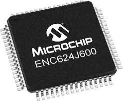
ENC624J600-I/PT microcontroller: Datasheet, Features, Application[FAQ]2023-03-07
ATMEGA1280-16AU microcontroller: Datasheet, Features, Application[FAQ]2023-03-07
STM8S207CBT6 Microcontroller: Datasheet, Features, Application[FAQ]2023-03-06
2N7002P Mosfet: Datasheet, Pinout, Features [FAQ]2021-10-21
L298N Motor Driver: Datasheet, Arduino, Circuit [Video&FAQ]2021-10-21