info@kynix.com
 00852-6915 1330


 0
0





TVS and eFuse Coordination for 24 V Industrial Inputs: Calculating Clamping Limits and Surge Margins
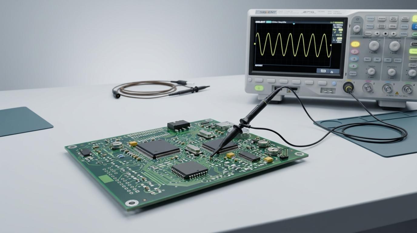
This engineering guide provides industrial hardware, power, and EMC engineers with a quantitative methodology for coordinating transient voltage suppression (TVS) diodes and electronic fuses (eFuses) on 24 V DC power inputs. Coordinating front-end surge protection requires balancing two conflicting physical boundaries: maintaining reverse standoff voltage above continuous rail swells at sub-zero temperatures, and restricting dynamic surge clamping below the eFuse pass-FET absolute maximum voltage rating at elevated junction temperatures. Relying on nominal datasheet peak pulse power ratings (PPP) routinely causes catastrophic lab failures during IEC 61000-4-5[1] testing. Applying dynamic resistance calculations, combination-wave generator source impedance analysis, and localized inductive kickback mitigation establishes a mathematically verified protection window.Industrial 24 V Boundary Conditions: Defining the Voltage WindowIndustrial 24 V DC input protection requires setting the TVS minimum breakdown voltage above the highest steady-state input swell across the entire operating temperature range to prevent thermal runaway.Boundary CategoryParameterValue / ConditionOperational BandNominal input window19.2 V to 28.8 V (IEC 61131-2 continuous)Operational BandMax swell / ripple30.2 V (upper steady-state boundary)TVS StandoffVRWM selection≥ 30.0 V to 33.0 VTVS BreakdownVBR(min) at −40°CMust exceed 30.2 VSurge Clamping Band (IEC 61000-4-5, 1 kV / 2 Ω)VC(surge) at +105°C — standard TVS55 V to 68 VSurge Clamping Band (IEC 61000-4-5, 1 kV / 2 Ω)VC(surge) at +105°C — flat-clamp TVS38 V to 41 VeFuse Maximum RatingsTier 1 VIN(AMR)≤ 40 V to 42 V (breached by standard TVS)eFuse Maximum RatingsTier 2 VIN(AMR)55 V to 67 V (compliant with standard TVS)IEC 61131-2 Supply Tolerances and Continuous Voltage SwellsUnder IEC 61131-2[2] (and EN 61131-2), standard industrial 24 V DC supply rails require a continuous steady-state operational tolerance of −15%/+20%, defining an operating window of 19.2 V to 28.8 V DC. However, real-world plant distribution networks introduce additional continuous variables, such as:Three-phase full-wave rectification rippleLine regulation slumpsDynamic load-dump recovery swellsThese variables push the upper continuous envelope to 30.0 V−30.2 V DC.Consequently, selecting a TVS diode with a reverse standoff voltage (VRWM) matched purely to the nominal 24 V rail (such as a 24 V device with VBR(min)≈26.7 V) is a critical failure mode. When the industrial supply swells to 28.8 V or 30.2 V, a 24 V TVS enters its conduction knee. The resulting continuous current dissipation quickly causes thermal runaway, shorting the input rail to ground and blowing upstream power supplies. Therefore, the absolute lower operational boundary for the TVS standoff voltage must satisfy:VRWM≥30.0 V(ideally 33.0 V)Temperature Derating Physics on TVS Breakdown VoltageSilicon avalanche TVS junctions possess a positive temperature coefficient of breakdown voltage (αT), typically between +0.08% and +0.091%/∘C. While high temperatures increase the breakdown voltage, sub-zero ambient operating environments contract it.For an industrial control system rated to operate down to −40∘C (ΔT=−65∘C relative to the standard calibration point of +25∘C), the minimum breakdown voltage (VBR(min)) drops by approximately $5.5\%$ to $6.0\%$:VBR(min)(−40∘C)=VBR(min)(+25∘C)×[1+αT×(−40−25)]If an engineer selects a TVS with an initial +25∘C breakdown voltage of 31.1 V (typical of an SMCJ28A), the breakdown voltage drops to approximately 29.3 V at −40∘C. If the industrial bus simultaneously operates at its upper continuous tolerance of 30.2 V, the device experiences false breakdown during cold-start operations.To guarantee that the TVS draws only negligible leakage current (IR≤1 μA−5 μA) across all environmental states, the standoff margin condition must be satisfied:Marginstandoff=VBR(min)(−40∘C)−VIN\_continuous(max)>0 VDynamic Clamping Physics: Deconstructing the Peak Pulse Power RatingA TVS diode rated for 1500 W fails to protect a 40 V eFuse because high surge currents drive the diode's internal dynamic resistance, forcing the clamping voltage far above its nominal breakdown knee.The Pulse Width Mismatch: 10/1000 μs vs. IEC 61000-4-5 8/20 μsA frequent source of circuit failure is assuming that a 600 W or 1500 W TVS rating guarantees protection against an IEC 61000-4-5 surge event[1]. The headline peak pulse power figure (PPP) on a TVS datasheet is specified against a slow 10/1000 μs current impulse (10 μs rise time, 1000 μs decay to half-value), historically used in telecommunications standards.Conversely, the IEC 61000-4-5 Combination Wave Generator (CWG) delivers:An open-circuit voltage impulse of 1.2/50 μsA short-circuit current impulse of 8/20 μsThe CWG presents a distinct source impedance depending on the coupling network:Differential mode (Line-to-Line): Coupled via an 18 μF capacitor with an internal generator source impedance of Rsource=2 Ω.Common mode (Line-to-Earth): Coupled via a 9 μF capacitor in series with an additional 10 Ω resistor, yielding an effective impedance of Rsource=12 Ω.Because an 8/20 μs pulse is fifty times shorter than a 10/1000 μs pulse, the silicon junction can absorb significantly higher peak current before thermal destruction. However, higher current through the junction creates a proportionally higher voltage drop across the device's internal bulk silicon resistance.Dynamic Resistance (Rdyn) and Clamping CalculationIn the avalanche breakdown region, the clamping voltage across the TVS is not a static ceiling. It is a linear function governed by the junction's dynamic resistance (Rdyn):VC(IPP)=VBR(nom)+IPP·RdynDynamic resistance can be extracted from the high-current slope of the datasheet IV curves[7] or derived from nominal pulse ratings:Rdyn≈VC(max)−VBR(min)IPP(datasheet)For standard 1500 W surface-mount TVS diodes (such as the SMCJ series), Rdyn typically ranges between 0.15 Ω and 0.25 Ω.Consider an industrial 24 V port subjected to an IEC 61000-4-5 Level 2 differential surge of 1 kV through the standard 2 Ω generator impedance, protected by a standard 33 V TVS (e.g., SMCJ33A, VBR(min)=36.7 V, Rdyn≈0.18 Ω):Surge Current Calculation: Assuming an initial clamp voltage estimate of VC≈60 V, the peak surge current delivered by the generator into the low-impedance shunt is:IPP≈Vsurge−VCRsource+Rparasitic=1000 V−60 V2 Ω+0.05 Ω≈458.5 AActual Dynamic Clamping Voltage: Feeding this current back into the dynamic resistance equation yields:VC=36.7 V+(458.5 A×0.18 Ω)≈119.2 V(theoretical unconstrained)In reality, standard SMC packaging cannot sustain 450 A without immediate bond-wire fusion or severe silicon clipping. However, even when current-sharing with supply line impedance drops IPP down to 120 A−150 A, the resulting clamp voltage reaches:VC=36.7 V+(150 A×0.18 Ω)≈63.7 VAt elevated junction temperatures (+105∘C), positive thermal coefficients push this clamping level beyond 68 V.TVS clamping voltage rise driven by dynamic resistance under 8/20 µs surge currentThe eFuse Vulnerability Mechanism: Why OVLO Does Not Protect VINA widespread misconception is that selecting an eFuse equipped with internal Overvoltage Lockout (OVLO) or dynamic overvoltage clamping eliminates the need for strict TVS clamping coordination.An eFuse integrates an internal charge pump, control logic, current sense amplifier, and an internal high-side pass-FET (typically an N-channel MOSFET). When an overvoltage event occurs, the internal OVLO comparator detects the rising edge and charges down the pass-FET gate within 100 ns to 500 ns, isolating the downstream system load (VOUT) from the input rail.Node in Simplified Input StagePhysical ConnectionExposure During SurgeIN+ terminal / primary shuntTVS diode to GND, CIN to GNDFull incoming transient, shunted by TVSeFuse VIN pin / pass-FET drainHardwired to incoming power traceClamped voltage VC appears directly herePass-FET source / VOUTIsolated when OVLO tripsProtected from transient once FET opensDownstream loadConnected to VOUT and COUTIsolated from transient by pass-FET cutoffHowever, the eFuse's own VIN pin, gate driver bias circuitry, and the drain terminal of the internal pass-FET remain physically hardwired to the incoming power trace. Turn-off isolates the load, but the entire clamping voltage appears directly across the eFuse's input silicon. If the TVS clamping voltage (VC) exceeds the pass-FET drain-to-source absolute maximum rating (VIN(AMR)), the eFuse experiences instantaneous avalanche or dielectric oxide breakdown. The device typically fails as a permanent drain-to-source short circuit, destroying both the protection IC and the downstream electronics it was selected to isolate.Candidate Screening Matrix: TVS and eFuse Coordination Framework for 24 V InputReliable TVS eFuse coordination for 24V input lines requires matching the TVS peak dynamic clamping voltage to the eFuse input absolute maximum rating with at least a 10% safety margin.Classification of Industrial eFuse Voltage TiersIndustrial eFuses divide into two primary categories based on input voltage capability:Tier 1 (Narrow Voltage Margin / Legacy Switches): VIN(AMR)≤36 V−42 V. These devices are designed for tightly regulated supplies. When deployed on 24 V industrial lines, they provide zero tolerance for unmitigated surge clamping.Tier 2 (High-Voltage Surge-Rated Switches): VIN(AMR)=55 V−67 V (with transient ratings up to 70 V). Devices in this category (such as the STMicroelectronics STEF01 rated for 55 V AMR, or the Texas Instruments TPS2663[6] rated for 60 V operating and 67 V AMR) are engineered to absorb the residual clamping voltages of standard industrial TVS diodes.TVS Device CategoriesStandard Zener TVS (SMAJ, SMBJ, SMCJ Series): Economical and widely available, but characterized by moderate dynamic resistance (Rdyn≈0.15 Ω−0.35 Ω), producing elevated clamping voltages under high surge currents.High-Power Surface-Mount TVS (DO-218AB Footprint, e.g., SM8S Series): Designed for automotive and heavy-industrial transient applications. Large silicon die sizes reduce dynamic resistance (Rdyn<0.08 Ω), keeping clamping lower under heavy current stress.Active Flat-Clamp Devices (e.g., TI TVS3300): Integrated solid-state suppressors that utilize an active feedback topology to achieve a steep, vertical clamping characteristic, dropping dynamic resistance to near-zero values past the breakdown knee.Industrial 24 V Coordination MatrixThe following matrix evaluates candidate combinations against an IEC 61000-4-5 Level 2 (1 kV open-circuit / 2 Ω source impedance) differential surge event across an industrial temperature range (−40∘C to +105∘C).TVS Device Class / ExampleContinuous Standoff (VRWM)Min Breakdown at −40∘C (VBR(min))Clamping at 8/20 μs Peak Surge (VC(max) at +105∘C)Compatibility with Tier 1 eFuse (VIN(AMR)≤40 V)Compatibility with Tier 2 eFuse (VIN(AMR)≥60 V)Failure Mode / Engineering AssessmentUnder-rated Zener (e.g., SMCJ24A)24.0 V25.2 V42.5 V (@40 A)FAILFAILThermal Runaway: Premature breakdown occurs during normal 28.8 V−30.2 V line swells. TVS short-circuits to ground during steady-state operation.Standard 28 V Zener (e.g., SMCJ28A)28.0 V29.4 V52.0 V−58.0 V (@100 A)FAILMARGINALOverstress Hazard: VBR drops below 30.2 V line swell at −40∘C. Clamping breaches Tier 1 AMR by >12 V and leaves minimal margin for 60 V eFuses.Standard 33 V Zener (e.g., SMCJ33A)33.0 V34.7 V60.5 V−68.0 V (@150 A)FAILPASS (with 67 V−70 V transient eFuse)Robust Baseline: Avoids all operational line swell conduction. Clamping destroys Tier 1 eFuses, but aligns safely with Tier 2 (e.g., TPS2663) 67 V ratings.High-Power DO-218AB (e.g., SM8S33A)33.0 V34.8 V54.5 V (@120 A)FAILPASS (High Safety Margin)Heavy Industrial Standard: Lower dynamic resistance maintains tighter clamping envelope. Exceeds Tier 1 limits, but provides >12 V margin for Tier 2 switches.Precision Flat-Clamp (e.g., TVS3300)33.0 V34.5 V38.5 V−41.0 V (@35 A)CONDITIONALPASS (Maximum Margin)Narrow Window Solution: Extremely flat clamping profile keeps surge voltage near 40 V. Requires upstream resistance if surge current exceeds 35 A−40 A.The Golden Coordination RulesFor any TVS and eFuse pairing to achieve certification without empirical guesswork, two mathematical conditions must be simultaneously satisfied:Marginstandoff=VBR(min)(−40∘C)−VIN\_continuous(max)>0 VMarginclamping=VIN(AMR)−VC(surge)(IPP,+105∘C)≥0.10×VIN(AMR)Circuit Architecture Solutions for Narrow MarginsWhen component constraints prevent the TVS clamping voltage from naturally falling below the eFuse absolute maximum rating, hardware engineers must implement series decoupling impedance, migrate to high-voltage silicon, or neutralize fast-trip inductive spikes.Coordinating with Series Decoupling ImpedanceWhen design constraints mandate the use of a Tier 1 eFuse (VIN(AMR)≤40 V) alongside a standard 33 V standoff TVS, the voltage differential (ΔV≈20 V−28 V) must be dropped across a series decoupling element positioned between the TVS and the eFuse input terminal.Series Resistor (Rseries): Inserting a flameproof, surge-rated resistor of 0.5 Ω to 2.0 Ω creates a transient voltage divider with the internal impedance of the eFuse's input bypass capacitor. Under high-frequency surge edges, the resistor limits peak current into the eFuse pin, allowing a secondary, low-power clamping device (such as a small SMAJ33A or precision clamp) located directly at the eFuse pin to clip residual voltage without absorbing primary pulse energy.Trade-off: Continuous I2R power dissipation during normal operation (Ploss=Iload2·Rseries) restricts this technique to lower-current industrial branches (typically Iload≤2 A).Series Inductor (Lseries): Replacing the resistor with a pulse-withstanding inductor (10 μH to 47 μH) provides frequency-dependent attenuation without DC power dissipation. The inductor impedes the rapid rise-time of the 8/20 μs current wave (VL=L·didt), forcing the primary TVS to absorb the surge while keeping the downstream eFuse input voltage below its absolute maximum rating.Trade-off: Requires shielded components with saturation currents (Isat) well above peak operating current to avoid core saturation during surge events.Migrating to Tier 2 Industrial eFusesFor industrial systems handling loads above 3 A, adding series resistance is thermally prohibitive, and high-current surge inductors require substantial PCB volume. The preferred architecture migrates the power switch to a dedicated Tier 2 high-voltage industrial eFuse.Devices such as the Texas Instruments TPS2663 offer a continuous operating range up to 60 V and an absolute maximum input rating of 67 V DC (withstanding dynamic transients up to 70 V). Pairing an SMCJ33A or SM8S33A with a 67 V AMR eFuse creates an integrated protection block:The TVS handles the bulk energy of the IEC 61000-4-5 pulse, clamping the rail to ≈58 V−64 V.The eFuse absorbs this residual voltage safely below its 67 V threshold.Downstream sub-systems remain fully isolated because the eFuse's internal adjustable overvoltage cutoff limits output voltage to user-configured levels (e.g., clamping or cutting off at 30 V).Managing Inductive Kickback (L·di/dt) During Fast TripDuring a severe short-circuit or surge event, the eFuse fast-trip comparator acts to isolate the pass-FET, interrupting large fault currents in under 100 ns to 500 ns.This extreme rate of current decay (didt) interacts with parasitic cable and PCB trace inductance (Ltrace) located between the power entry connector and the eFuse input terminal. The resulting inductive kickback voltage superimposes on the incoming DC rail:Vspike=−Ltrace·didtFor example, a trace inductance of only 40 nH experiencing an interruption of a 30 A fault in 200 ns generates:Vspike=40×10−9 H×(30 A200×10−9 s)=6.0 VIf the input rail is already sitting at the TVS clamping ceiling of 62 V, this inductive transient pushes the peak input voltage to 68 V, puncturing an eFuse rated for 65 V−67 V AMR.Layout Rule: Place the primary TVS diode immediately adjacent to the input connector pins to shunt incoming surge energy before it couples into the board plane. In addition, place a local, low-ESR ceramic bypass capacitor (CIN≥1.0 μF−4.7 μF, X7R, rated for ≥100 V) directly across the eFuse VIN and $GND$ pins, within 2 mm of the silicon package. This local capacitor provides a low-impedance sink for the inductive current trapped in trace inductance when the pass-FET opens, eliminating inductive kickback spikes.Bench Verification and Electrical Test ProtocolsValidating surge margin requires measuring component breakdown voltages, dynamic pulse clamping profiles, and post-stress silicon leakage currents under controlled lab conditions.Breakdown or Clamping Voltage Testing of a 6600W Transient Voltage Suppression (TVS) DiodePre-Test TVS Parameter VerificationBefore subjecting prototypes to destructive surge injection, verify the actual breakdown characteristics and terminal polarity of the physical protection diodes.Bench Polarity Verification: On high-power automotive and industrial surface-mount TVS diodes (such as the DO-218AB package), terminal assignments differ from standard low-power axial diodes. In uni-directional DO-218AB devices, the large exposed copper heatsink tab is the Anode, while the bent clip lead is the Cathode.Reversing this footprint places the TVS in forward bias across the incoming supply rails. In forward mode, the silicon junction clamps the rail to a standard diode drop of 0.520 V, creating a dead short that destroys the TVS or pulls down the bench power supply upon initial power-up. In reverse polarity verification with a digital multimeter in diode-check mode, the display must read open loop (O.L.).Bench Measurement of VBR Without Curve Tracers: Engineers can verify the breakdown knee (VBR) of a TVS diode using a standard programmable DC bench power supply:Configure the DC power supply strictly to Constant Current (CC) mode, setting the compliance current limit exactly to the datasheet test current:IT=5 mA(0.005 A)Set the open-circuit voltage limit higher than the expected maximum breakdown voltage (e.g., set voltage to 45 V for a 33 V TVS).Connect the supply across the TVS in reverse bias (positive terminal to Cathode, negative to Anode).Safety Rule: Never test breakdown in uncapped constant voltage mode. Stepping an unregulated voltage source past the breakdown knee will draw massive current due to near-zero dynamic resistance, instantly destroying the diode or triggering power supply crowbar shutdowns.When energized, the power supply will transition into constant-current regulation (5 mA). The resulting voltage readout displayed on the supply terminals represents the actual room-temperature VBR at IT. For an SMCJ33A, this value should settle within the 36.7 V to 40.6 V specification window.Expert Nuance: A diode that measures 36.8 V on a bench supply at 5 mA has not established its surge clamping limit. In visual stress tests, devices clamping at 36.8 V under a 5 mA bench excitation routinely scale past 60 V when driven by 150 A combination wave surges due to internal Rdyn. The bench test confirms junction integrity and manufacturing tolerance, not surge-level clamping immunity.Bench verification of TVS breakdown voltage and DO-218AB terminal polarityIEC 61000-4-5 Surge Injection and Probing ArchitectureSurge testing must be conducted using a calibrated Combination Wave GeneratorReferencesIEC 61000-4-5: Electromagnetic compatibility (EMC) - Part 4-5: Testing and measurement techniques - Surge immunity test — International Electrotechnical CommissionIEC 61131-2: Industrial-process measurement and control - Programmable controllers - Part 2: Equipment requirements and tests — International Electrotechnical CommissionTransient protection design for power switches to achieve robust, reliable power-path protection — Texas InstrumentsDemystifying Surge Protection — Texas InstrumentsTVS Surge Protection in High-Temperature Environments — Texas InstrumentsTPS2663x 60-V, 6-A Power Limiting, Surge Protection Industrial eFuse Datasheet — Texas InstrumentsTransient Voltage Suppressors (TVS Diode) Applications Overview — Littelfuse Inc.AN1977: Transient Voltage Suppressors: Operation and Features — Renesas Electronics Corporation
On 2026-09-12