 info@kynix.com
 00852-6915 1330


 0
0


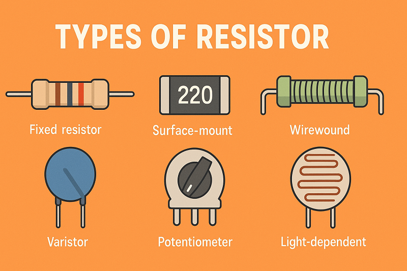
IntroductionIn modern compact circuit board designs, have you ever been puzzled by how to efficiently implement multiple identical or related resistor functions while saving valuable PCB space and ensuring parameter consistency? As electronic products become increasingly miniaturized and complex, traditional discrete resistor solutions often fall short, not only increasing wiring difficulty but also introducing unnecessary parasitic effects and temperature drift differences. This is precisely why network resistors (also known as “resistor arrays”) [Wikipedia] have emerged as the ideal choice for engineers. They cleverly integrate multiple resistors into a single package, offering a perfect solution to the aforementioned challenges. You can learn more about pull-up and pull-down resistors at [Kynix]. Additionally, if you are interested in circuit design, you can refer to [Kynix’s Transistor Common-emitter Amplifier Circuit Design Guide].This article will start with the most valuable user queries, providing you with a comprehensive understanding of network resistors’ application scenarios, core calculation methods, working principles, and practical guides for selection, simulation, and fault diagnosis. Whether you are a newcomer to the electronics field or an experienced engineer, this authoritative guide will help you thoroughly master network resistors, bringing revolutionary improvements to your designs. You can find more information about electronic components at [Kynix].Video 1: Introduction to Resistor Networks (Source: YouTube)1 Core Applications of Network Resistors: Why and Where to Use ThemNetwork resistors hold a significant position in modern electronic design precisely because they can efficiently and reliably solve various circuit design challenges. They are not merely simple collections of resistors but crucial components for optimizing space and enhancing performance. You can learn more about resistor types and their applications at [Kynix]. Let’s delve into the core applications of network resistors in different scenarios.1.1 Pull-up and Pull-down Resistor NetworksIn digital circuits, especially in microcontroller (MCU) I/O ports and various bus communications (e.g., I2C, SPI), the signal line’s voltage state needs to be clearly defined. When no external signal is driving, the signal line may be in an undefined “floating” state, leading to abnormal system behavior. At this point, pull-up resistors (connecting the signal line to a high level) or pull-down resistors (connecting the signal line to a low level) become particularly important. Network resistors offer significant advantages in this application:Simplified Wiring: When multiple I/O pins or bus lines require pull-up/pull-down, a single network resistor can replace multiple discrete resistors, greatly reducing the number of components on the PCB and simplifying wiring complexity.Ensuring Consistent Pin Levels: Since resistors within a network resistor are typically manufactured using the same process, they exhibit excellent matching, ensuring highly consistent pull-up/pull-down characteristics for multiple signal lines. This is crucial for the stability of multi-channel parallel signals or bus communications.1.2 Signal Line Termination ResistorsIn high-speed digital signal transmission, such as DDR memory buses, Ethernet, or LVDS signal lines, signal integrity is a core design challenge. When a signal encounters impedance mismatch at the end of a transmission line, signal reflection occurs, leading to waveform distortion, increased bit error rates, and even system crashes. The role of termination resistors is to absorb these reflected signals, ensuring clear signal transmission.Network resistors, as termination resistor arrays, can provide:Preventing Signal Reflection: By precisely matching the characteristic impedance of the transmission line, signal reflection is effectively suppressed, maintaining the integrity of the signal waveform.Ensuring Signal Integrity: Especially in multi-channel parallel high-speed signal lines, using network resistors can ensure consistent matching characteristics for all lines, thereby improving the signal integrity and reliability of the entire system.1.3 Voltage Divider NetworksVoltage divider networks are one of the most common applications in electronic circuits, used to precisely scale down a higher voltage to a lower voltage. This is very common in applications such as digital-to-analog converter (DAC) outputs, reference voltage generation, and sensor signal conditioning. Network resistors offer unique advantages in voltage divider applications:Precise Resistor Ratios: Due to the consistency of the manufacturing process, the ratio accuracy between resistors within a network resistor is much higher than that of discrete resistors. This is crucial for applications requiring high-precision voltage output.Good Temperature Tracking: When temperature changes, the resistance values of all resistors within a network resistor change in a similar manner. This means their relative ratios remain constant, ensuring the stability of the voltage division ratio and reducing the impact of temperature on circuit performance.1.4 LED Current Limiting Resistor ArraysIn applications requiring the driving of multiple LED indicators or LED displays, each LED typically needs a current-limiting resistor to protect it from excessive current. If discrete resistors are used, PCB space will be quickly occupied, and the assembly process will become cumbersome. Network resistors provide an elegant solution:Saving PCB Space: A single network resistor can replace multiple independent current-limiting resistors, significantly reducing the required circuit board area, which is particularly important for miniaturized product designs.Simplifying Assembly Process: The integrated package makes component placement and soldering more efficient, reducing production costs and error rates.Pro Tip: When selecting network resistors for LED current limiting, always consider the rated power of each resistor to ensure it can withstand the LED’s operating current and avoid overheating damage.2 Resistor Network Calculation and Analysis TechniquesUnderstanding the working principles of network resistors requires precise calculation and analysis of their internal resistor networks [DigiKey]. This is not only the foundation of theoretical learning but also an indispensable skill in practical circuit design. This section will delve into basic calculation methods, advanced analysis techniques, and recommended simulation tools for resistor networks.2.1 Basics: Equivalent Resistance CalculationWhether for discrete resistors or connections within network resistors, calculating equivalent resistance is at the core of circuit analysis. Mastering the formulas and techniques for series, parallel, and mixed networks is fundamental to understanding complex resistor networks. You can learn more about comparisons of resistors in series and in parallels at [Kynix].Series Resistors: When resistors are connected end-to-end, and current flows sequentially through each resistor, they form a series circuit. The total equivalent resistance is the sum of all series resistor values. For example, if R1, R2, and R3 are in series, then R_eq = R1 + R2 + R3.Parallel Resistors: When both ends of resistors are connected to the same points in a circuit, they form a parallel circuit. The reciprocal of the total equivalent resistance is the sum of the reciprocals of all parallel resistors. For example, if R1, R2, and R3 are in parallel, then 1/R_eq = 1/R1 + 1/R2 + 1/R3.Mixed Networks: In practical circuits, combinations of series and parallel connections are common. When calculating, you typically start from the innermost series or parallel sections and gradually simplify until the entire network is reduced to a single equivalent resistor.Important Note: For network resistors, their internal connection method (isolated, bussed) determines how their equivalent resistance is calculated. For example, the common terminal of a bussed resistor array can usually be considered a single node, and the resistors on the other pins form a parallel relationship with this node.Equivalent Calculation Diagram for Series, Parallel, and Mixed Resistor NetworksFigure 1: Equivalent Calculation Diagram for Resistor Networks (Source: DZSC.com)2.2 Advanced Analysis TechniquesFor more complex and large resistor networks that cannot be simply simplified by series and parallel combinations, we need more powerful analysis tools. Star-Delta (Y-Δ) transformation, nodal voltage method, and mesh current method are powerful tools for solving such problems.Star-Delta (Y-Δ) Transformation: This is a mathematical tool used to simplify complex resistor networks. When a circuit contains a “bridge” structure that is neither purely series nor purely parallel, Y-Δ transformation can convert a star connection (Y-shape) into an equivalent delta connection (Δ-shape), and vice versa, allowing the entire network to be simplified for calculation. This is particularly useful when analyzing certain sensor bridge circuits or complex power distribution networks.Nodal Voltage Method: This is a systematic analysis method based on Kirchhoff’s Current Law (KCL). It selects one node in the circuit as a reference point (usually ground) and then sets up KCL equations with the voltages of other nodes as unknowns. By solving these equations, the voltages of all nodes in the circuit can be obtained, and then the current and power of any branch can be calculated. The nodal voltage method is very efficient for complex networks containing multiple voltage and current sources.Mesh Current Method: Similar to the nodal voltage method, the mesh current method is a systematic analysis method based on Kirchhoff’s Voltage Law (KVL). It defines independent meshes in the circuit (closed loops that do not contain other meshes) and assumes a circulating current in each mesh. By setting up KVL equations for each mesh and solving for the mesh currents, the currents in all branches of the circuit can ultimately be obtained. The mesh current method excels in analyzing circuits containing multiple resistors and voltage sources.2.3 Practical Tools: Recommended Resistor Network Simulation SoftwareIn modern electronic design, manually calculating complex resistor networks is both time-consuming and prone to errors. Simulation software has become an invaluable aid for engineers, enabling them to quickly and accurately analyze circuit behavior and optimize designs.LTspice: A free, high-performance SPICE simulation software provided by Analog Devices. It is powerful, supporting the simulation of various analog circuits and switching power supplies, including complex resistor networks. LTspice has a vast component library and a relatively intuitive user interface, making it the preferred tool for many engineers for circuit verification and troubleshooting.Multisim: A popular circuit simulation software developed by National Instruments. Multisim provides an intuitive graphical interface and supports the simulation of digital, analog, and mixed-signal circuits. It integrates virtual instruments, allowing it to simulate oscilloscopes, multimeters, etc., making it very suitable for teaching and rapid prototyping.How to Use Software for Resistor Network Circuit Simulation and Analysis:Build the Circuit: Drag and drop components in the simulation software, connecting network resistors and other components according to the actual circuit diagram.Set Parameters: Set the correct resistance values, tolerances, temperature coefficients, and other parameters for the network resistors.Run Simulation: Select the appropriate simulation type (e.g., DC operating point analysis, transient analysis, AC analysis, etc.) and run the simulation.Analyze Results: View simulation results in the form of waveforms, reports, etc., to verify circuit functionality, analyze voltage and current distribution, and evaluate the performance of network resistors under different conditions.Pro Tip: When performing simulations, try changing the parameters of the network resistors (e.g., resistance value, topology) and observe the changes in circuit response. This will help you gain a deeper understanding of their impact on overall circuit performance.Video 2: How to Calculate Series and Parallel Resistor Combination Circuits (Source: YouTube)Video 3: Resistor Network Analysis and Circuit Simulation using LTspice (Source: YouTube)3 Working Principles and Selection of Network ResistorsTo truly master network resistors, a deep understanding of their working principles and the correct selection methods is crucial. This will not only help you maximize their advantages in design but also avoid potential problems.3.1 Unveiling the Working Principles of Network Resistors3.1.1 Basic Definition: What is a Network Resistor (Resistor Array)?Network resistors, commonly known as “resistor arrays,” are electronic components that integrate multiple independent or interconnected resistor elements into a single package. Unlike individual discrete resistors, resistor arrays are designed to provide a compact, efficient, and consistent resistor array to meet the demands for miniaturization, high integration, and high reliability in modern electronic circuits. They ensure high matching accuracy and excellent temperature tracking characteristics between internal resistors through precise manufacturing processes. You can find more resistor products at [Kynix].3.1.2 Detailed Explanation of Internal TopologiesThe internal connection method of network resistors is key to their functional versatility. According to different application requirements, resistor arrays are mainly divided into the following topologies:Isolated Type: This type of resistor array contains multiple completely independent resistors, each with two independent pins. There are no electrical connections between them. Isolated resistor arrays are suitable for applications requiring multiple independent resistors but also aiming to save space and simplify assembly, such as independent current limiting or voltage division for multiple signals.Internal Structure Diagram of Isolated Resistor ArrayFigure 2: Internal Structure Diagram of Isolated Resistor Array (Source: DZSC.com)Bussed Type: Bussed resistor arrays are the most widely used type. One end of all internal resistors is connected to a common pin (usually marked with a dot or special symbol on the resistor array), while the other ends are independently routed out. This structure is very suitable for pull-up/pull-down resistor networks, LED current-limiting arrays, and other applications that require multiple components to be connected to a common power supply or ground. Its advantage lies in greatly simplifying PCB wiring and ensuring consistent electrical characteristics between all resistors and the common point.Internal Structure Diagram of Bussed Resistor ArrayFigure 3: Internal Structure Diagram of Bussed Resistor Array (Source: RS Components)Dual-Terminator Type: This is a special type of network resistor, usually consisting of two series resistors forming a voltage divider, and providing multiple sets of such voltage dividers within the same package. Its main feature is extremely high matching accuracy and temperature tracking performance between internal resistors, making it very suitable for applications requiring precise voltage division or termination matching, such as differential signal termination matching for data buses.3.1.3 Introduction to Manufacturing Processes and MaterialsThe manufacturing process of network resistors plays a decisive role in their performance. Currently, mainstream manufacturing technologies include:Thick Film Technology: This is the most common manufacturing process. Resistor paste (containing conductive materials, glass powder, and organic binders) is printed on a ceramic substrate and then fired at high temperatures to form the resistive layer. Thick film resistors are characterized by low cost, wide resistance range, and high reliability, but their precision is relatively low.Thin Film Technology: Through vacuum deposition (such as sputtering or evaporation), a very thin layer of resistive material (such as nickel-chromium alloy) is deposited on a ceramic or silicon substrate. Thin film resistors offer higher precision, better temperature stability (lower TCR), and lower noise, but at a relatively higher cost.3.2 High-Precision Network Resistor Selection GuideSelecting the appropriate network resistor is crucial for ensuring circuit performance. Here are the key technical parameters to focus on during selection:3.2.1 Interpretation of Key Technical ParametersResistance Value and Tolerance:Resistance Value: Refers to the nominal resistance value of each resistor inside the network resistor, usually in ohms (Ω).Tolerance: Represents the maximum allowable deviation between the actual resistance value and the nominal resistance value, usually expressed as a percentage (e.g., ±1%, ±5%). For high-precision applications, a resistor array with a smaller tolerance should be selected.Temperature Coefficient (TCR):TCR (Temperature Coefficient of Resistance): Describes the extent to which the resistance value changes with temperature, usually in ppm/°C (parts per million per degree Celsius). A smaller TCR value indicates better temperature stability of the resistor. For precision circuits, especially those operating over a wide temperature range, low TCR network resistors are essential. This is a significant differentiating advantage of network resistors compared to discrete resistors, as resistors within the same package have similar TCRs and exhibit good temperature tracking.Rated Power and Package Thermal Resistance:Rated Power: Refers to the maximum power that the network resistor can continuously dissipate at a specified ambient temperature. When selecting, ensure that the actual power consumption of each resistor does not exceed its rated power, and allow for sufficient margin.Package Thermal Resistance: Represents the package’s ability to conduct internal heat to the external environment. Lower thermal resistance indicates better heat dissipation. In densely packed or high-power applications, special attention should be paid to thermal resistance to avoid overheating.Resistance Ratio Matching and Tracking TCR:Ratio Matching: This is one of the core advantages of network resistors. It refers to the relative resistance accuracy between different resistors within the same package. For example, if a 10kΩ and 1kΩ resistor pair has a ratio matching of 0.1%, it means the accuracy of their ratio (10:1) is as high as 0.1%. This is extremely important for applications like voltage dividers and differential amplifiers that rely on resistance ratios rather than absolute values.Tracking TCR: Refers to the difference in TCR between different resistors within the same package. Due to manufacturing consistency, the resistance values of resistors within a network resistor change in a very similar trend when temperature changes, thus maintaining a highly stable ratio. This is an indispensable feature for precision measurement and signal processing circuits.3.2.2 Package Specifications: SMD and Through-Hole (DIP/SIP) ReferenceNetwork resistors are available in various package forms to suit different assembly needs and space constraints:SMD (Surface Mount Device):Features: Small size, light weight, suitable for automated production, and the mainstream choice for modern compact electronic products.Common Packages: For example, 0402x4 (meaning 4 resistors of 0402 size integrated into one package), 0603x8, etc. These packages usually have smaller pin pitches and require more precise soldering processes. You can find more SMD resistors/chip resistors at [Kynix].SMD Resistor Array ExampleFigure 4: SMD Resistor Array Example (Source: CSDN Blog)Through-Hole Devices:DIP (Dual In-line Package):Features: Pins are arranged in two rows and can be directly inserted into PCB holes for soldering. Easy for manual soldering and prototyping, but occupies more space.Applications: Commonly found in older electronic products, educational experiment boards, or applications where space is not a critical concern.SIP (Single In-line Package):Features: Pins are arranged in a single row, saving more PCB space than DIP and simplifying wiring.Applications: Often used in situations requiring vertical mounting to save horizontal space, such as memory modules or certain specific function modules.Pro Tip: When choosing a package, in addition to considering space and assembly methods, also pay attention to the package’s impact on heat dissipation. Although SMD packages are small, they may require additional heat dissipation design in high-power applications.4 Fault Diagnosis and Advanced TopicsEven highly reliable network resistors can fail under extreme conditions or after prolonged use. Understanding common failure modes and correct diagnostic procedures is crucial for quickly pinpointing problems and repairing circuits. Additionally, this section will explore some advanced topics related to resistor networks to broaden your horizons.4.1 Network Resistor Fault Diagnosis Process4.1.1 Common Failure ModesNetwork resistor failures typically manifest in the following modes:Open Circuit: This is one of the most common failures, characterized by a broken internal connection within the resistor, preventing current flow. In the circuit, this manifests as related functions failing, such as LEDs not lighting up or abnormal signal line levels. Open circuits can be caused by burnout due to overcurrent, mechanical stress, or manufacturing defects.Short Circuit: Relatively less common, but if it occurs, it can lead to excessive current in the circuit and even damage other components. Short circuits are usually caused by internal insulation failure or accidental connections between pins.Resistance Drift: The resistance value deviates from the nominal value, which may lead to degraded circuit performance or abnormal functionality. Resistance drift is usually caused by prolonged operation in high-temperature, high-humidity environments, or by electrical or mechanical stress, leading to degradation of the resistive material’s properties.4.1.2 Diagnostic Flowchart: From Visual Inspection to Multimeter MeasurementWhen a network resistor is suspected of failure, the following diagnostic procedure can be followed:Visual Inspection:First, visually inspect the network resistor for obvious physical damage, such as burn marks, cracks, deformed pins, or corrosion. These signs usually indicate overcurrent or overheating issues.Check if the solder joints are firm and free of cold joints or dry joints.Multimeter Measurement:Power Off Operation: Before taking any measurements, ensure that the circuit is completely powered off and all charges are discharged to avoid electric shock or damage to the multimeter.Measure Individual Resistors: For isolated resistor arrays, you can directly measure the resistance across each resistor. For bussed resistor arrays, you need to find the common terminal and then measure the resistance between the common terminal and each independent pin.Compare with Nominal Value: Compare the measured resistance value with the nominal value on the network resistor. If the measured value is much larger than the nominal value (usually infinite), it may be an open circuit; if the measured value is much smaller than the nominal value (close to 0Ω), it may be a short circuit; if the measured value deviates significantly from the nominal value (outside the tolerance range), it may be resistance drift.Check Common Terminal: For bussed resistor arrays, you can use the multimeter’s continuity test (buzzer) to check if the common terminal is conductive with all independent pins and if the independent pins are insulated from each other.In-Circuit Testing (Proceed with Caution):In some cases, if power cannot be turned off, you can try in-circuit measurement. However, please note that in-circuit measurements may be affected by other components in the circuit, leading to inaccurate results. Therefore, in-circuit measurement results are for reference only, and final confirmation still requires off-circuit measurement.4.1.3 Solution: How to Correctly Replace and Soldering PrecautionsOnce a network resistor failure is confirmed, it needs to be replaced. Correct replacement and soldering operations are crucial for ensuring circuit reliability: You can learn more about basic electronic components at [Kynix].Select the Correct Replacement: Ensure that the replacement network resistor’s model, resistance value, tolerance, power, and package type are identical to the original component. If the original component is obsolete, carefully consult the datasheet to select a compatible replacement in terms of electrical characteristics and physical dimensions.Desoldering: Carefully remove the faulty component using an appropriate soldering iron and desoldering wick or hot air gun. Avoid damaging the PCB pads.Clean Pads: After removing the component, thoroughly clean any residual solder and flux from the pads, ensuring they are clean and flat.Soldering:Orientation: For directional resistor arrays (e.g., bussed type), always install them according to the markings on the PCB or the datasheet instructions. The common terminal usually has a dot or chamfer mark.Temperature and Time: Use appropriate soldering temperature and time to avoid overheating damage to the component or PCB. For SMD components, reflow soldering or a hot air gun is recommended.Solder Amount: Ensure an appropriate amount of solder is used to form full, shiny solder joints, free of cold joints, short circuits, or dry joints.Inspection: After soldering, visually inspect again and use a multimeter to measure the newly installed network resistor to confirm its proper functionality.4.2 Advanced Topics: Distributed Networks and Noise4.2.1 Introduction to Resistor Distributed Network ModelsIn some high-frequency or precision applications, simply treating a resistor as a lumped element may no longer be accurate. When the signal frequency is very high, or the physical size of the resistor is comparable to the signal wavelength, the distributed effects of the resistor (such as parasitic capacitance and parasitic inductance) become significant. At this point, we need to introduce the resistor distributed network model.A distributed network model treats a resistor as a transmission line composed of countless tiny series resistors and parallel capacitors (or inductors). This model is very important when analyzing high-speed signal transmission, RF circuits, or power integrity issues. For example, even purely resistive traces on a PCB will exhibit transmission line characteristics at high frequencies, requiring a distributed model to analyze their impedance, reflection, and loss.4.2.2 Introduction to Resistor Network Noise AnalysisAny resistor, no matter how precise, generates noise. In precision measurement and low-noise applications, analyzing resistor network noise is crucial. Resistor noise primarily includes:Thermal Noise: Also known as Johnson noise or Nyquist noise, it is caused by the random thermal motion of electrons in a conductor. Thermal noise is inherent to all resistors and cannot be eliminated. Its magnitude is related to temperature, bandwidth, and resistance value. The formula is $V_n = \sqrt{4kTRB}$, where k is Boltzmann’s constant, T is the absolute temperature, R is the resistance value, and B is the bandwidth.Shot Noise: In semiconductor devices, noise generated due to the randomness of charge carriers passing through a potential barrier. In some types of resistors, if there is a PN junction or similar structure, shot noise may also be generated.Flicker Noise (1/f Noise): Also known as 1/f noise, its power spectral density is inversely proportional to frequency. Flicker noise is more significant at low frequencies and is usually related to material defects, surface effects, and current flow. In precision DC or low-frequency measurements, flicker noise is the primary noise source.When designing low-noise circuits, it is necessary to:Select Low-Noise Resistors: Thin film resistors generally have lower noise than thick film resistors.Optimize Resistance Value: Select an appropriate resistance value to minimize thermal noise while meeting circuit functionality.Limit Bandwidth: Limit the circuit’s bandwidth through filtering or other means to reduce noise.Consider Temperature: Lowering the operating temperature can effectively reduce thermal noise.5 Conclusion and Frequently Asked Questions (FAQ)5.1 SummaryThrough this in-depth discussion, we can clearly see that **network resistors (resistor arrays) [TrustedParts.com] are far from simple collections of resistors; they are indispensable precision components in modern electronic design. They demonstrate significant advantages in improving circuit integration, consistency, and reliability, making them an ideal choice for addressing space constraints and signal integrity challenges.We started from the core applications of network resistors, understanding their unique value in pull-up/pull-down networks, signal termination matching, precise voltage division, and LED current limiting. Subsequently, we mastered the basic calculation methods and advanced analysis techniques for resistor networks and learned the importance of simulation tools in design verification. Finally, we delved into the working principles and internal topologies of network resistors and provided practical guides for high-precision selection and fault diagnosis.In summary, applications, calculations, and selection are the three pillars of mastering network resistors. Only by fully understanding these aspects can you unleash their full potential in actual projects. We encourage all engineers and designers to confidently choose network resistors in future circuit designs based on the strategies in this guide, as they will help you build more compact, stable, and efficient electronic systems.5.2 Frequently Asked Questions (FAQ)Q1: What is the fundamental difference between a network resistor and using multiple discrete resistors?A1: The main differences lie in size, cost, parasitic parameter consistency, and temperature tracking characteristics. Network resistors integrate multiple resistors into a single package, significantly saving PCB space and assembly costs. More importantly, due to the unified manufacturing process, their internal resistors exhibit excellent matching accuracy and temperature tracking characteristics, meaning their resistance ratios remain highly stable when temperature changes, which is an advantage discrete resistors can hardly match.Q2: How do I identify the orientation (first pin) on a network resistor?A2: Typically, it is identified by a marking dot or chamfer on the package. For example, many DIP or SIP package network resistors will have a circular indentation or a chamfered corner near the first pin. For SMD packages, silk screen markings may also indicate the orientation. Before actual use, always refer to the datasheet of the corresponding model to avoid incorrect connection.Q3: Which pin is the common terminal of a bussed network resistor?A3: The common terminal of a bussed network resistor is usually the pin marked with a dot or special symbol. This pin connects to one end of all internal resistors. For example, in an 8-pin bussed resistor array, pin 1 or pin 8 is usually the common terminal. Again, the most accurate identification method is to consult the datasheet for that specific model.Q4: Are all resistors in a network resistor array the same value?A4: Within a single package, all resistors have the same nominal resistance value. For example, a network resistor with a nominal value of 10kΩ will have each internal resistor designed to be 10kΩ. However, the actual values may fluctuate within their tolerance range. While the absolute value of individual resistors may vary slightly, the core advantage of network resistors lies in their excellent ratio matching and tracking TCR between internal resistors, which is crucial for circuit designs that rely on resistance ratios.Q5: In which scenarios do network resistors offer greater advantages than discrete resistors?A5: Network resistors offer greater advantages in the following scenarios: when saving PCB space is required (e.g., miniaturized products); when simplifying wiring and assembly processes is needed; when the circuit has high requirements for resistor matching accuracy and temperature tracking characteristics (e.g., precision voltage division, signal termination matching, DAC reference voltage); and when driving multiple identical loads (e.g., LED current-limiting arrays). In these cases, network resistors can provide higher integration, better performance consistency, and lower overall cost.Further ReadingResistor - WikipediaIntroduction to Precision Resistor Networks - Texas InstrumentsUnderstanding Resistor Arrays: Technical Principles, Application Scenarios, and Manufacturer Selection Strategies - EET-China
On 2025-08-11


