 info@kynix.com
 00852-6915 1330


 0
0


")

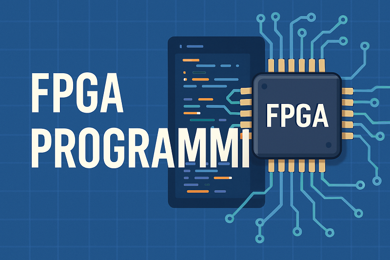
IntroductionIn the rapidly evolving landscape of high-performance computing and embedded systems, Field-Programmable Gate Arrays (FPGAs) have emerged as a cornerstone technology, offering unparalleled flexibility and acceleration capabilities. Among the titans of this industry, Intel FPGA (formerly Altera) stands out, providing a robust portfolio of programmable logic devices that power everything from data centers to cutting-edge AI applications. Have you ever wondered how these versatile chips are shaping the future of technology, or perhaps felt overwhelmed by the sheer complexity of getting started with FPGA development? You’re not alone. The world of FPGAs can seem daunting, but understanding Intel’s offerings, especially since its acquisition of Altera, is crucial for anyone looking to leverage hardware acceleration.Did you know that the global FPGA market is projected to reach over $12 billion by 2027, driven by the increasing demand for AI, 5G, and IoT applications? This growth underscores the critical role FPGAs play in modern technological advancements. This comprehensive guide will demystify Intel FPGA (Altera), walking you through its core technologies, development tools, product lines, and ecosystem. We’ll explore everything from fundamental concepts to advanced applications, providing a clear roadmap for both beginners and experienced engineers. By the end of this article, you’ll have a solid understanding of Intel FPGA’s capabilities and how to navigate its powerful ecosystem to accelerate your next project.Figure 1: An Intel FPGA development board, showcasing various components and interfaces.Source: The Samtec BlogIntel FPGA vs Xilinx (AMD): Architecture, Performance, and Ecosystem ShowdownWhen diving into the world of FPGAs, the perennial debate between Intel FPGA and Xilinx (now AMD) is unavoidable. Both companies offer powerful, albeit distinct, approaches to programmable logic. While Intel FPGAs, with their roots in Altera, are often lauded for their strong emphasis on embedded processors and system-on-chip (SoC) designs, Xilinx has historically focused on high-performance logic and advanced DSP capabilities. This rivalry has driven innovation, providing developers with a rich choice of architectures tailored for diverse applications.Figure 2: An Intel FPGA chip, highlighting its compact design and processing power.Source: WebWireLet’s break down some key comparisons across their product lines:Intel FPGA Cyclone vs Xilinx Spartan ComparisonFor cost-sensitive and low-power applications, both Intel and Xilinx offer entry-level FPGA families. Intel’s Cyclone series, such as the Intel FPGA Cyclone V and Cyclone 10 LP, are popular choices for their balance of logic, memory, and I/O capabilities, often found in industrial, automotive, and consumer electronics. On the other hand, Xilinx’s Spartan series, including the Spartan-7, provides a compelling alternative with a focus on general-purpose logic and connectivity. While both aim for economic viability, subtle differences in their fabric and toolchain can influence design choices.FeatureIntel FPGA Cyclone SeriesXilinx Spartan SeriesTarget Use CasesIndustrial, Automotive, Consumer, Low-Power EmbeddedGeneral-Purpose Logic, Connectivity, Cost-OptimizedKey StrengthsIntegrated hard IP, SoC capabilities (Cyclone V SoC)DSP slices, flexible I/O, broad ecosystemPower EfficiencyGood for low-power applicationsCompetitive, especially for general logicFigure 3: A comparative overview of significant FPGA product families from Intel, Xilinx, and Lattice Semiconductor.Source: JAK ElectronicsIntel FPGA Arria vs Xilinx Artix/Kintex ComparisonMoving up the performance ladder, Intel’s Arria series and Xilinx’s Artix/Kintex families compete in the mid-range to high-performance segments. Intel FPGA Arria devices, like the Arria 10, are designed for high-bandwidth applications, featuring high-speed transceivers and DSP blocks, making them suitable for communications, broadcast, and military applications. Xilinx’s Artix-7 and Kintex-7 (and their Ultrascale counterparts) offer a strong proposition with their emphasis on DSP performance and high-speed serial connectivity, often preferred in medical imaging, test & measurement, and aerospace.Intel FPGA Stratix vs Xilinx Virtex/Versal ComparisonAt the pinnacle of FPGA performance, Intel’s Stratix series and Xilinx’s Virtex/Versal families battle for dominance in the most demanding applications. Intel FPGA Stratix devices, such as the Stratix 10 and the newer Agilex series, push the boundaries of performance with advanced process technologies, high-density logic, and integrated features like HBM (High Bandwidth Memory) and advanced transceivers. These are deployed in data centers, high-performance computing (HPC), and 5G infrastructure. Xilinx’s Virtex UltraScale+ and the adaptive compute acceleration platform (ACAP) Versal series offer formidable competition, integrating powerful processing systems, AI engines, and advanced connectivity for next-generation systems. The choice here often hinges on specific workload requirements, power budgets, and the intricacies of their respective development ecosystems.Figure 4: The user interface of Intel Quartus Prime Software, showing project creation options.Source: Intel.comPro Tip: When comparing FPGAs, always look beyond raw logic element counts. Consider the number and type of DSP blocks, embedded memory, transceiver speeds, and the availability of hard IP blocks relevant to your application. The true performance lies in how these resources are integrated and optimized for your specific design.Intel FPGA Software & Toolchain: Quartus Prime Core GuideDeveloping with FPGAs requires a robust and intuitive software suite, and for Intel FPGAs, that suite is primarily the Quartus Prime Software. This comprehensive multiplatform environment provides everything you need to design, synthesize, simulate, and program FPGAs, SoC FPGAs, and CPLDs. It’s the central hub for your FPGA development journey, offering a rich set of features that streamline the design flow from concept to silicon.Quartus Prime comes in different editions (Lite, Standard, and Pro), catering to various design complexities and device families. Key features include an advanced synthesis engine, timing analysis tools, power analysis, and the Qsys system integration tool, which significantly accelerates the process of connecting IP blocks and creating complex systems-on-chip. For instance, Qsys allows you to visually assemble your system, automatically generating the interconnect logic, saving countless hours of manual HDL coding.Intel Nios II Embedded Processor Introduction and PracticeOne of the significant advantages of the Intel FPGA ecosystem is the Intel Nios II embedded processor. This is a highly configurable, royalty-free 32-bit embedded soft-core processor that you can implement within your FPGA. It allows you to integrate a microcontroller-like functionality directly into your hardware design, enabling hybrid hardware-software solutions on a single chip. This is particularly useful for control logic, data processing, and managing peripherals that don’t require the extreme parallelism of the FPGA fabric.Figure 5: A block diagram illustrating the configurable components of the Intel Nios II Processor.Source: FPGA loverGetting started with Nios II typically involves:Hardware Design: Using Qsys to instantiate the Nios II processor and connect it to various peripherals (GPIO, UART, timers, custom IP).Software Development: Writing C/C++ code using the Nios II Embedded Design Suite (EDS), which is based on the Eclipse IDE. This allows you to develop firmware that runs on the Nios II processor.Debugging: Utilizing the integrated debugging tools within EDS to test and verify your software on the FPGA.The Nios II processor significantly simplifies the development of complex embedded systems by allowing a portion of the design to be handled in software, leveraging familiar programming paradigms while still benefiting from the hardware acceleration capabilities of the FPGA.Accelerating Development with Intel FPGA HLS CompilerTraditional FPGA development often involves writing hardware description languages (HDLs) like Verilog or VHDL, which can be time-consuming and complex for high-level algorithms. This is where the Intel FPGA HLS (High-Level Synthesis) Compiler comes into play. HLS allows designers to describe their algorithms in C++ and then automatically synthesize that C++ code into optimized RTL (Register Transfer Level) for implementation on an FPGA.Figure 6: An Altera MAX 10 FPGA Development Board, ideal for beginners and cost-effective projects.Source: Amazon.comBenefits of using the Intel FPGA HLS Compiler include:Increased Productivity: Develop at a higher level of abstraction, significantly reducing design and verification time.Faster Exploration: Quickly iterate on architectural choices and explore different implementations to find the optimal balance of performance, area, and power.Software-Hardware Co-design: Bridge the gap between software and hardware development teams, enabling software engineers to contribute directly to FPGA designs.IP Reuse: Easily reuse C++ intellectual property (IP) across different projects and platforms.While HLS offers tremendous advantages, it’s important to understand the nuances of writing synthesizable C++ code to achieve efficient hardware. It’s a powerful tool for accelerating complex algorithm implementation on FPGAs, especially for applications like digital signal processing and machine learning.Verilog for Intel FPGA Best PracticesEven with the advent of HLS, Verilog (and VHDL) remains fundamental to FPGA design. Adhering to best practices when writing Verilog for Intel FPGAs ensures efficient resource utilization, better timing closure, and easier debugging. Here are some key considerations:Synchronous Design: Prioritize synchronous design principles, using a single clock domain for most logic and carefully managing clock domain crossings (CDCs).Reset Strategy: Implement proper reset synchronization to avoid metastability issues.Blocking vs. Non-Blocking Assignments: Understand and correctly use blocking (=) and non-blocking (<=) assignments. Non-blocking assignments are generally preferred for sequential logic to avoid race conditions.Finite State Machines (FSMs): Use clear and concise coding styles for FSMs, separating combinational and sequential logic for readability and synthesis.Parameterization: Utilize parameters to create flexible and reusable modules.Avoid Latches: Be mindful of inferring latches, as they can lead to unpredictable behavior and are generally discouraged in synchronous designs.Testbenches: Develop comprehensive testbenches to thoroughly verify your Verilog modules before hardware implementation.Important Note: While the Quartus Prime software provides powerful synthesis capabilities, well-written and optimized HDL code will always yield better results. Familiarize yourself with the Intel FPGA design guidelines and coding styles for optimal performance and resource usage.Intel FPGA Development Board Selection and Procurement GuideChoosing the right Intel FPGA development board is a critical step in your design journey. These boards provide a ready-to-use hardware platform, allowing you to quickly prototype, test, and validate your FPGA designs without the need for custom PCB fabrication. Intel and its partners offer a wide array of development kits, ranging from low-cost options for beginners to high-performance platforms for complex applications.Figure 7: An Intel MAX 10 FPGA Development Kit, showcasing its compact design and integrated features.Source: Intel.comWhen selecting a development board, consider the following factors:FPGA Family: Match the board’s FPGA (e.g., Cyclone, Arria, Stratix, MAX 10) to your project’s performance, power, and cost requirements.On-board Peripherals: Look for peripherals relevant to your application, such as DDR memory, Ethernet, USB, HDMI, cameras, or specialized connectors.Connectivity: Ensure the board offers the necessary I/O interfaces and expansion options (e.g., FMC, PMOD, Arduino headers).Development Tools Support: Verify compatibility with Intel Quartus Prime Software and other necessary tools.Community and Documentation: A strong community and comprehensive documentation can significantly ease the learning curve and debugging process.For beginners, boards based on the Intel MAX 10 or Cyclone series are often recommended due to their lower cost and simpler architecture. For more advanced projects, Arria or Stratix-based boards provide higher logic density, faster transceivers, and more integrated features.Intel FPGA Pricing Strategy and Cost AnalysisUnderstanding the pricing of Intel FPGAs can be complex, as it varies significantly based on device family, logic density, features, and volume. Generally, FPGAs are priced higher than ASICs (Application-Specific Integrated Circuits) for high-volume production due to their reconfigurability and flexibility. However, for low-to-medium volume production, rapid prototyping, or applications requiring field upgrades, FPGAs offer a compelling cost advantage.Intel employs a tiered pricing strategy, with entry-level devices like the MAX 10 and Cyclone series being the most budget-friendly, while high-end Stratix and Agilex devices command premium prices due to their cutting-edge performance and advanced features. It’s important to consider not just the chip cost, but also the total cost of ownership, which includes development board expenses, software licenses (though Quartus Prime Lite is free), and engineering time.Recent trends indicate potential price adjustments in the FPGA market. For instance, some reports suggest Intel Altera may implement price increases in certain product categories in early 2025. When procuring FPGAs or development boards, it’s often beneficial to work with authorized distributors who can provide competitive pricing, volume discounts, and technical support.Official and Third-Party Intel FPGA Distributor DirectoryProcuring genuine Intel FPGA products and development boards from authorized sources is crucial to ensure authenticity, quality, and access to technical support. Intel maintains a network of official distributors globally. These distributors not only supply the hardware but also often provide valuable pre-sales and post-sales support, training, and design services.Some of the major authorized distributors for Intel (and formerly Altera) FPGAs include:Arrow Electronics: A global provider of electronic components and enterprise computing solutions. Arrow.comMouser Electronics: Specializes in the rapid introduction of new products and technologies for design engineers. Mouser.comDigi-Key Electronics: Offers a vast selection of electronic components for immediate shipment. DigiKey.comAvnet: A global technology distributor and solutions provider. Avnet.comAdditionally, many third-party vendors and academic partners offer specialized development boards and kits that integrate Intel FPGAs. While these can be excellent for specific use cases or educational purposes, always verify the vendor’s reputation and support before purchase.Intel FPGA Power Management Solutions ExplainedPower management is a critical aspect of FPGA design, especially for high-performance devices and battery-powered applications. Intel FPGA devices incorporate advanced power management features and require careful consideration of power delivery networks (PDN) to ensure stable operation and optimal performance. Efficient power management can significantly reduce operating costs and extend battery life in portable devices.Key aspects of Intel FPGA power management solutions include:Power Rails: FPGAs typically require multiple voltage rails for core logic, I/O, transceivers, and memory interfaces. Each rail needs a stable and clean power supply.Power Estimation Tools: Intel provides tools like the Power and Thermal Calculator (PTC) to estimate power consumption early in the design cycle, allowing engineers to optimize their designs for power efficiency.Dynamic Power Management: Modern Intel FPGAs, such as the Agilex series, feature advanced power-optimization capabilities like SmartVID, which dynamically adjusts core voltage to reduce power consumption while maintaining performance.Power Delivery Network (PDN) Design: Proper PDN design, including decoupling capacitors and PCB layout, is essential to minimize voltage droop and noise, ensuring reliable operation of the FPGA.External Power Management ICs (PMICs): Often, external PMICs from companies like Infineon or Monolithic Power Systems (MPS) are used in conjunction with FPGAs to provide efficient and regulated power delivery.Designing for low power is more important than ever, and Intel provides extensive documentation and support resources to help designers implement robust power management solutions for their FPGA-based systems.How to Start Learning Intel FPGA from Scratch: A RoadmapEmbarking on the journey of learning Intel FPGAs can be both exciting and challenging. With a solid roadmap, however, you can navigate the learning curve and build a strong foundation in FPGA development. Whether you’re a student, a hobbyist, or a professional looking to expand your skillset, here’s a step-by-step guide to get you started.Master the Fundamentals: Before diving into FPGAs, ensure you have a good grasp of digital logic concepts, including Boolean algebra, logic gates, flip-flops, and state machines. A solid understanding of these fundamentals is crucial for successful FPGA design.Learn an HDL: Choose a Hardware Description Language (HDL) to learn. Verilog and VHDL are the two most common HDLs. While both are powerful, Verilog is often considered to have a syntax that is more familiar to C programmers.Get a Development Board: As mentioned earlier, a development board is essential for hands-on learning. The Terasic DE10-Lite or DE10-Nano are excellent and affordable choices for beginners, featuring Intel MAX 10 and Cyclone V FPGAs, respectively.Install Quartus Prime: Download and install the free Intel Quartus Prime Lite Edition software. This will be your primary tool for designing, synthesizing, and programming your FPGA.Start with Simple Projects: Begin with classic “Hello, World!” projects for FPGAs, such as blinking an LED or controlling a seven-segment display. These simple projects will help you get familiar with the Quartus Prime workflow.Explore Tutorials and Resources: Leverage the vast amount of online resources available. Intel provides extensive documentation, tutorials, and training materials. Additionally, websites like FPGA developer and communities on Reddit (r/FPGA) are great places to learn and ask questions.What is Altera FPGA? A Brief History and Current StatusTo understand Intel FPGA, it’s essential to know its history with Altera. Founded in 1983, Altera was a pioneer in the programmable logic industry, introducing the world’s first reprogrammable logic device in 1984. For over three decades, Altera was a major player in the FPGA market, competing fiercely with Xilinx.In 2015, Intel acquired Altera for $16.7 billion, a landmark deal that integrated Altera’s leading FPGA technology with Intel’s processor and manufacturing prowess. Initially, the Altera brand was phased out in favor of “Intel FPGA.” However, in a strategic move in early 2024, Intel announced that it would operate its FPGA division as a standalone company named Altera, an Intel Company. This rebranding aims to provide the FPGA business with more autonomy and focus, allowing it to better serve its customers and accelerate innovation in the programmable solutions market.“By separating our FPGA business, we can create a more focused and agile organization that is better positioned to capitalize on the significant growth opportunities in the FPGA market.” - Sandra Rivera, CEO of AlteraOfficial and Community Tutorial Resources for Intel FPGAThere is a wealth of tutorial resources available for learning Intel FPGA. Here are some of the best places to find them:Intel FPGA Academic Program: Intel offers a dedicated program for students and educators, providing access to development boards, software, and course materials. Intel FPGA Academic ProgramIntel FPGA YouTube Channel: The official Intel FPGA YouTube channel features numerous tutorials, webinars, and product demonstrations.Terasic Website: Terasic, a major manufacturer of Intel FPGA development boards, provides excellent tutorials and resources for their products.Online Learning Platforms: Websites like Coursera, Udemy, and edX offer courses on FPGA design and Verilog/VHDL programming.OpenVINO on Intel FPGA: Deploying AI Inference ApplicationsOne of the most exciting applications of modern FPGAs is in the field of Artificial Intelligence (AI). OpenVINO (Open Visual Inference & Neural Network Optimization) toolkit is a comprehensive suite of tools from Intel that helps developers optimize and deploy AI inference workloads across a range of Intel hardware, including FPGAs. By leveraging OpenVINO, you can accelerate deep learning models on Intel FPGAs, achieving high performance and low latency for applications like computer vision, natural language processing, and robotics.The workflow for deploying AI on an Intel FPGA with OpenVINO typically involves:Training a Model: Train a deep learning model using a popular framework like TensorFlow or PyTorch.Optimizing with Model Optimizer: Use the OpenVINO Model Optimizer to convert the trained model into an Intermediate Representation (IR) that is optimized for Intel hardware.Deploying with Inference Engine: Use the Inference Engine to run the optimized model on the FPGA, taking advantage of its parallel architecture for high-throughput inference.Detailed Explanation of Intel MAX 10 Series CPLD/FPGAThe Intel MAX 10 series deserves a special mention as it blurs the line between CPLDs (Complex Programmable Logic Devices) and FPGAs. These devices offer the non-volatile, instant-on benefits of a CPLD with the density and features of a low-cost FPGA. This unique combination makes them ideal for a wide range of applications, including system control, I/O expansion, and power management.Key features of the Intel MAX 10 series include:Dual-Configuration Flash: Allows for dynamic switching between two different FPGA configurations.Analog Blocks: Integrated ADCs (Analog-to-Digital Converters) and temperature sensors.Nios II Soft-Core Processor Support: Enables the implementation of a soft-core processor for embedded control.Single-Chip Solution: The non-volatile nature of the MAX 10 eliminates the need for an external configuration device, saving board space and cost.These features make the Intel MAX 10 a versatile and cost-effective choice for many designs, and a great starting point for those new to the world of FPGAs.ConclusionNavigating the world of Intel FPGA (Altera) reveals a rich and powerful ecosystem that is integral to modern technology. From the cost-effective MAX 10 and Cyclone series to the high-performance Stratix and Agilex families, Intel offers a comprehensive portfolio of programmable logic devices to meet the demands of a wide range of applications. The acquisition of Altera has solidified Intel’s position in the FPGA market, blending its processor expertise with Altera’s programmable logic leadership. As we’ve explored, the journey into FPGA development is made accessible through powerful tools like Quartus Prime Software, the flexibility of the Nios II embedded processor, and the productivity gains of the Intel FPGA HLS Compiler.As the demand for AI, 5G, and high-performance computing continues to grow, the role of FPGAs will only become more critical. Intel’s strategic focus on this area, highlighted by the re-emergence of the Altera brand, signals a renewed commitment to innovation and customer success. Whether you are a seasoned engineer looking to accelerate your next design or a newcomer eager to dive into the world of programmable logic, the resources and technologies within the Intel FPGA ecosystem provide a clear path forward. The future of hardware is flexible, and with Intel FPGAs, you have the tools to build it.Ready to start your FPGA journey? Explore the official Intel FPGA website for the latest product information, download the Quartus Prime Lite Edition for free, and check out our wide selection of Intel FPGA development boards to find the perfect platform for your next project.Further ReadingXilinx vs. Intel: A Deep Dive into the FPGA GiantsGetting Started with Verilog: A Beginner’s GuideThe Role of FPGAs in Accelerating AI WorkloadsHave you ever found yourself at a crossroads, unsure which FPGA path to take for your project?Choosing the right FPGA can be a daunting task, especially with the myriad of options available from Intel and other vendors. Many engineers, like Sarah, a hardware startup founder, initially struggled with optimizing their designs for both performance and cost. “We spent weeks trying to port our algorithm to an ASIC, only to realize an FPGA could give us the flexibility we needed for rapid iteration,” she recounts. “The learning curve was steep, but with Intel’s Quartus Prime and their extensive documentation, we were able to get our prototype up and running much faster than anticipated.”Another common challenge is power management. John, an embedded systems developer, shared his experience: “Our initial design was consuming too much power, and we were hitting thermal limits. It wasn’t until we delved into Intel’s power estimation tools and applied their SmartVID features that we managed to significantly reduce our power footprint without compromising performance. It was a game-changer for our battery-powered device.”Common Pitfalls When Buying Intel FPGAsWhile Intel FPGAs offer immense potential, there are several common traps to avoid during the procurement and design process:Underestimating Software Costs: While Quartus Prime Lite is free, the Pro Edition and certain IP cores can incur significant licensing fees. Always factor these into your budget.Ignoring Power Management: Neglecting proper power delivery network (PDN) design and power optimization techniques can lead to unstable operation, thermal issues, and reduced device lifespan.Overlooking Development Board Compatibility: Ensure the development board you choose is fully compatible with your target FPGA device and offers the necessary peripherals and expansion options for your project.Skipping Community Resources: The FPGA community is a treasure trove of knowledge. Failing to leverage forums, online tutorials, and open-source projects can lead to unnecessary delays and frustration.Not Considering Long-Term Support: Verify the availability of long-term support, errata, and updates for your chosen FPGA family, especially for products with extended lifecycles.How to Choose the Best Intel FPGA for You: A Buying ChecklistTo simplify your decision-making process, consider this checklist:Define Your Requirements: What are your project’s performance, power, and cost targets? What kind of logic density, memory, and I/O are needed?Evaluate FPGA Families: Research Intel’s Cyclone, Arria, Stratix, and MAX 10 series to find the best fit for your application.Assess Development Tools: Ensure you are comfortable with the Quartus Prime software and its features, including HLS and Nios II if applicable.Check Ecosystem Support: Look for available IP cores, reference designs, and community support for your chosen device.Consider Power Budget: Use Intel’s power estimation tools to ensure your design meets power consumption goals.Review Pricing and Availability: Compare prices from authorized distributors and consider lead times.Editor’s ReviewFrom my personal experience working with various FPGA platforms, Intel FPGAs (and their Altera heritage) consistently deliver on performance and reliability. The integration of hard IP blocks, particularly in their SoC FPGAs, significantly simplifies complex designs. While the learning curve for Quartus Prime can be steep for newcomers, the depth of its features and optimization capabilities is truly impressive. The Nios II processor is a fantastic addition, allowing for flexible hardware-software co-design. For anyone serious about hardware acceleration, especially in areas like AI inference or high-bandwidth data processing, investing time in the Intel FPGA ecosystem is highly rewarding. The recent re-emphasis on the Altera brand also signals a positive direction, promising more focused innovation and support for the FPGA community.Frequently Asked Questions (FAQ)Is Intel FPGA the same as Altera?Yes, Intel FPGA is the same as Altera. Intel acquired Altera in 2015. While initially rebranded as “Intel FPGA,” the company recently announced it would operate its FPGA division as a standalone entity named Altera, an Intel Company, signaling a return to the well-known brand.What software is used for Intel FPGAs?The primary software used for Intel FPGAs is the Intel Quartus Prime Software. It provides a complete design environment for FPGAs, SoC FPGAs, and CPLDs, including design entry, synthesis, simulation, and programming.Which Intel FPGA is best for beginners?For beginners, the Intel MAX 10 series FPGAs are highly recommended. Development boards featuring MAX 10 devices, such as the Terasic DE10-Lite, are cost-effective and offer a good balance of features for learning the fundamentals of FPGA design.Can I use Verilog with Intel FPGAs?Yes, you can absolutely use Verilog (and VHDL) with Intel FPGAs. These Hardware Description Languages (HDLs) are fundamental to FPGA design, and the Intel Quartus Prime Software fully supports them for design entry and synthesis.How does OpenVINO relate to Intel FPGAs?OpenVINO is Intel’s toolkit for optimizing and deploying AI inference workloads across various Intel hardware, including FPGAs. It allows developers to accelerate deep learning models on Intel FPGAs, making them suitable for AI applications requiring high performance and low latency.
On 2025-08-30


