 info@kynix.com
 00852-6915 1330


 0
0


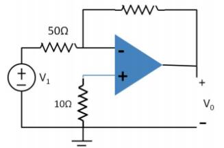
 when VSWR=3:1")
 when VSWR=3:1")
 changes in three kinds of circuits when VSWR=3:1")


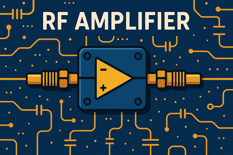
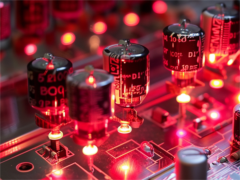
Rockford Fosgate, Alpine, Pioneer, Kicker, and Phoenix Gold stand out as top names in the world of rf amplifiers. Their popular amplifier models, both modern and vintage, set industry standards. Many buyers look for an rf amplifier that delivers high power output, strong reliability, and clear sound. The buyers guide highlights how each amplifier excels in different areas, such as performance or value. This buyers guide also compares rf amplifiers for sub amplifiers, ham radio, and professional audio. A good buyers guide gives every reader a fair review to help them pick the right amplifier. Comparison Criteria Power Output & Frequency Range Power output and frequency range define the core capabilities of rf amplifiers. Power output includes parameters such as saturated output power and the output 1 dB compression point, which indicate the maximum power the amplifier can deliver before distortion increases. Frequency range determines the amplifier’s ability to handle signals across different bands. Broadband amplifiers support multi-frequency operations, using advanced filtering to maintain signal integrity. Market data shows a 15% CAGR in the broadband amplifiers sector, reflecting their growing importance. Gain block amplifiers and variable gain amplifiers offer flexibility for both narrowband and broadband applications, ensuring optimal signal strength and coverage. Linearity & Sound Quality Linearity ensures that the rf amplifier reproduces input signals accurately, minimizing distortion. Key metrics include total harmonic distortion, third-order intercept point, and intermodulation distortion. These measurements validate the amplifier’s ability to maintain sound fidelity and signal clarity. Low noise amplifiers with excellent linearity provide superior sound quality, especially in high-fidelity audio and communication systems. Impedance matching and harmonic performance further enhance the overall sound experience. Reliability & Build Reliability and build quality impact the lifespan and consistent performance of rf amplifiers. Effective thermal management, using heat sinks and cooling fans, prevents thermal runaway and extends component life. Proper build can double the lifespan of an amplifier and reduce failure rates. High-quality construction ensures that broadband amplifiers and low noise amplifiers maintain stable operation even under demanding conditions. Features & User Interface Modern rf amplifiers offer features such as digital displays, remote controls, and user-friendly interfaces. Class d amplifier designs provide high efficiency and compact size, making them popular in portable and automotive applications. Class ab power amplifiers balance efficiency and sound quality, appealing to audiophiles. Gain block amplifiers and variable gain amplifiers allow users to adjust signal levels for different scenarios. Price & Value Price and value assessments consider both performance and long-term benefits. Detailed company profiles and benchmarking data help buyers compare rf amplifier models by price, features, and build quality. Market analysis tools, such as SPSS and Tableau, provide insights into competitive positioning and absolute dollar opportunities. Buyers should weigh price against value, considering both initial cost and the amplifier’s ability to deliver reliable power and sound over time. Low Noise Amplifiers Low noise amplifiers play a critical role in enhancing weak signals while minimizing noise. A good low noise amplifier achieves a noise figure around 1 dB and gain near 10 dB, ensuring clear signal reception. In advanced applications, such as 5G mm-wave, low noise amplifiers demonstrate noise figures between 2.3 dB and 2.5 dB with gain exceeding 25 dB. These amplifiers improve the signal-to-noise ratio, making them essential for high-performance rf amplifier systems. Broadband amplifiers and low noise amplifiers together support robust, high-quality communication and audio experiences. Leading RF Amplifier Brands Rockford Fosgate Rockford Fosgate has earned a strong reputation for powerful rf amplifier solutions. The brand focuses on sub amplifiers that deliver deep bass and clear sound. Many car audio enthusiasts choose Rockford Fosgate for its high quality build and reliable performance. The Punch and Power series stand out as top choices. Vintage models like the Punch 150HD remain popular for their robust design and high parts quality. Modern amplifiers from Rockford Fosgate use advanced technology to improve sound and efficiency. Alpine Alpine offers a wide range of rf amplifiers for both entry-level and professional users. The company is known for clean sound and user-friendly features. Alpine amplifiers often include digital controls and compact designs. Many users appreciate the high quality build and consistent performance. Vintage Alpine models, such as the V12 series, have a loyal following because of their clarity and reliability. Alpine continues to innovate with new amplifier models that meet the needs of today’s audio systems. Pioneer Pioneer stands as a leader in audio technology. The brand produces rf amplifier models that balance power and sound quality. Pioneer amplifiers work well in many applications, from car audio to home systems. The GM series and vintage models like the GM-120 show the company’s commitment to high quality sound. Pioneer uses advanced circuitry and strong build to ensure long-lasting performance. Kicker Kicker specializes in sub amplifiers that deliver strong bass and high output. The brand’s amplifiers are popular with users who want powerful sound in their vehicles. Kicker’s build quality and rugged design make its products reliable for daily use. The KX series and older models like the ZR series highlight Kicker’s focus on performance and durability. Many users trust Kicker for high power rf amplifier needs. Phoenix Gold Phoenix Gold is known for clarity and detailed sound. The brand’s amplifiers use high parts quality and careful build to achieve excellent audio performance. Vintage models such as the MS 275 are prized for their unique sound and craftsmanship. Phoenix Gold continues to develop new rf amplifier models that appeal to audiophiles and professionals. The company’s focus on sound quality and innovation sets it apart in the market. Best Power Amplifiers Choosing the best power amplifiers requires careful evaluation of technical specifications, sound quality, efficiency, and application fit. The following models represent the top choices from leading brands, each excelling in different areas of performance and technology. Rockford Fosgate Punch 150HD The Rockford Fosgate Punch 150HD stands as a classic example of high-quality power and reliability. This amplifier delivers robust output, making it a favorite among car audio enthusiasts who demand deep bass and clear signal reproduction. Pros: Delivers high power output with low distortion.Maintains signal clarity across the full frequency range.Durable build ensures long-term reliability. Cons: Larger size compared to modern compact amplifiers.Lacks advanced digital features found in newer models. Ideal Use Case:This model suits users who value classic sound and need reliable, high-quality power for subwoofers or full-range speakers in car audio systems. Phoenix Gold MS 275 Phoenix Gold’s MS 275 is renowned for its unique sound signature and craftsmanship. Audiophiles appreciate its detailed signal reproduction and smooth tonal balance. Specification / MetricDetailsPower Ratings75W x 2 @ 4Ω, 150W x 2 @ 2Ω (1% THD+N, RMS, 14.4V supply)Frequency Response10 Hz – 50 kHzSignal-to-Noise Ratio>100 dBAmplifier ClassABDistortion (THD+N)<0.03%BuildGold-plated terminals, premium internal components Pros: Exceptional sound clarity and low noise.High-quality power delivery with minimal distortion.Premium build and aesthetic appeal. Cons: Higher price point due to craftsmanship.Limited availability as a vintage model. Ideal Use Case:Best for audiophiles seeking the best power amplifiers for home or studio setups where sound detail and build quality matter most. Kicker Flagship Model Kicker’s flagship amplifier, such as the KX1200.1, offers high-efficiency power and rugged performance. It excels in delivering strong bass and handling demanding loads. Specification / MetricDetailsPower Ratings1200W x 1 @ 2Ω (1% THD+N, RMS, 14.4V supply)Frequency Response25 Hz – 200 HzSignal-to-Noise Ratio>95 dBAmplifier ClassDDistortion (THD+N)<0.5%BuildCompact, efficient cooling, durable enclosure Pros: High power output in a compact, high-efficiency design.Handles low-impedance loads with ease.Reliable for daily use in automotive environments. Cons: Focused frequency range limits use to subwoofers.Slightly higher distortion than Class AB models. Ideal Use Case:Perfect for users who need the best power amplifiers for subwoofer applications in vehicles, where space and efficiency are priorities. Alpine Top Model Alpine’s top amplifier, such as the PDX-V9, combines advanced technology with versatile performance. It provides high-quality power for both subwoofers and full-range speakers. Specification / MetricDetailsPower Ratings100W x 4 + 500W x 1 @ 4Ω (1% THD+N, RMS, 14.4V supply)Frequency Response5 Hz – 100 kHzSignal-to-Noise Ratio>105 dBAmplifier ClassDDistortion (THD+N)<0.05%BuildCompact, stackable, digital controls Pros: Delivers high-quality power to multiple channels.Wide frequency response supports detailed sound.Compact and stackable for flexible installations. Cons: Digital interface may require a learning curve.Premium price for advanced features. Ideal Use Case:Ideal for users seeking the best power amplifiers for multi-channel car audio systems, combining efficiency and sound quality. Pioneer Top Model Pioneer’s top amplifier, such as the GM-D9705, balances power, sound, and value. It uses advanced circuitry to maintain signal integrity and efficiency. Specification / MetricDetailsPower Ratings75W x 4 + 350W x 1 @ 4Ω (1% THD+N, RMS, 14.4V supply)Frequency Response10 Hz – 50 kHzSignal-to-Noise Ratio>100 dBAmplifier ClassDDistortion (THD+N)<0.05%BuildSleek, lightweight, efficient cooling Pros: Balanced sound with strong power output.Efficient design reduces heat and saves space.Competitive price for the feature set. Cons: Not as powerful as some dedicated sub amplifiers.Lacks some premium build features of higher-end models. Ideal Use Case:Great for users who want the best power amplifiers for both subwoofers and speakers, with a focus on value and versatility. Note: All listed models use standardized testing (ANSI/CTA-2006-D) for power ratings, frequency response, and distortion. High-precision analyzers ensure accurate measurement of signal quality and power output. Technology Differences: GaN and Amplifier Class GaN amplifiers operate at higher PWM switching frequencies (up to 800 kHz), producing near-ideal square wave output and reducing signal artifacts.These amplifiers achieve higher efficiency and generate less heat than traditional Class-A or Class-AB designs.GaN technology allows high power output in smaller, lighter packages, lowering manufacturing and shipping costs.GaN devices tolerate higher operating temperatures, especially when grown on SiC substrates, which improves reliability and high-quality power delivery.The telecom, automotive, and aerospace sectors drive GaN adoption for their ability to handle high-frequency and high-power signal applications.Class D amplifiers, often paired with GaN technology, offer high-efficiency operation, making them ideal for compact and energy-saving designs.Class AB amplifiers remain popular for their warm sound and low distortion, especially in vintage and audiophile models. Selecting the best power amplifiers involves balancing sound quality, power output, efficiency, and application needs. Most users find that amplifiers with 100 watts per channel provide sufficient power for typical listening environments. Matching amplifier and speaker quality ensures optimal system performance. Integrated amplifiers offer convenience, while separates allow for customization. Understanding the differences in amplifier class and technology helps users choose the best power amplifiers for their specific requirements. RF Amplifiers Comparison Table Model Specs The table below compares the main RF amplifier models from Rockford Fosgate, Phoenix Gold, Kicker, Alpine, and Pioneer. Each model offers unique strengths in power, frequency range, linearity, noise, features, and price. Note: All models use standardized testing for power and noise. Higher SNR means lower noise and better signal clarity. Performance & Value When comparing the best power amplifiers, each model excels in different areas. The Rockford Fosgate Punch 150HD and Phoenix Gold MS 275 both deliver strong power and low noise, making them top choices for sound quality. The Phoenix Gold MS 275 stands out for its superior linearity and noise performance, which appeals to audiophiles who want the cleanest signal. Kicker’s KX1200.1 provides high power for subwoofers, but its noise level is slightly higher due to its focus on output. Alpine’s PDX-V9 offers a wide frequency range and low noise, making it versatile for both subwoofers and speakers. Pioneer’s GM-D9705 balances power, noise, and price, giving users strong value for multi-channel setups. Statistical analysis, such as normalized mean-square error and weighted error-to-signal power ratio, helps engineers measure both linear and nonlinear distortion. These metrics, along with intercept points, show that the best power amplifiers maintain low noise and high signal accuracy across different loads. Engineers use advanced modeling, such as memory polynomial fitting and ANN-based models, to further improve amplifier performance and value. These methods help reduce noise and optimize signal quality for every application. Sound & Vintage Amplifiers Tube Amplifiers Vintage tube amplifiers continue to attract enthusiasts who value both craftsmanship and performance. Many collectors and audio professionals seek out brands like Premaluna and PS Audio for their attention to detail and robust construction. Tube amplifiers use vacuum tubes, also called valves, which can handle high voltages and withstand transient overloads. This durability made them essential in military and high-power RF applications during the Cold War. Some tubes operate at very high frequencies, even into the megahertz range, making them suitable for demanding RF tasks. Vacuum tubes can dissipate large amounts of heat, sometimes needing water cooling for high power transmitters.Tubes often run below their maximum voltage, which increases reliability and extends their lifespan.Nuvistor tubes, such as the 6CW4, work well for very high frequency amplification, reaching into UHF and microwave ranges.Frame-grid tubes use precise grid spacing to achieve high transconductance and low noise, improving the overall sound in RF amplifiers.Ceramic planar triodes, used in space and military gear, offer some of the lowest noise figures, which helps preserve sound quality at high frequencies. Tube amplifiers also exhibit softer clipping when overloaded. This trait creates a different distortion profile, which many listeners find pleasing in both RF and audio applications. Unique Sound Qualities Vintage and tube RF amplifiers deliver a sound that many describe as warm, rich, and full of character. Enthusiasts often praise the unique tonal qualities that tubes provide. Unlike modern solid-state amplifiers, tube designs introduce subtle harmonic distortion that enhances the listening experience. This effect gives music and signals a sense of depth and realism. Tube amplifiers produce a softer, more rounded sound when pushed to their limits.The noise performance of certain tubes, like the 7788 pentode in triode mode, rivals or surpasses many modern designs.Planar triodes can achieve near-zero noise figures at lower frequencies, preserving the purity of the sound.The construction and materials used in vintage amplifiers contribute to their distinctive sound signature. Collectors and professionals choose vintage tube amplifiers for their unmatched sound quality and the craftsmanship behind each unit. These amplifiers suit those who want a unique listening experience and value the history and engineering that shaped early RF technology. RF Amplifier Recommendations For Hobbyists Hobbyists often seek an amplifier that balances performance, ease of use, and affordability. The buyers guide highlights several models that deliver reliable power and low noise, making them ideal for entry-level users and radio enthusiasts. Many hobbyists prioritize low phase noise and stable frequency response, which ensures clear signals in transceiver setups. The table below compares popular amplifier models for hobbyists, focusing on phase noise—a key metric for signal clarity: The buyers guide also recommends these models for hobbyists: Ameritron ALS-600: Delivers 600W PEP output, covers 160-15 meter bands, and features a user-friendly design.Fairview Microwave FMAM5058: Offers 100W output, 50 dB gain, and a frequency range from 500 MHz to 1 GHz.ACOM 1200S-120: Provides 1000W output, covers 1.8 to 54 MHz, and includes automatic control.Fairview FMAM5110: Features 200W power saturation, 53 dB gain, and a frequency range from 20 MHz to 520 MHz. These amplifiers stand out for their practical performance metrics, such as power output, gain, and frequency coverage. Hobbyists benefit from easy integration and reliable operation. The buyers guide notes that envelope-tracking amplifiers help optimize efficiency and linearity, reducing distortion and improving signal quality. This balance is important for hobbyists who want dependable performance without complex setup. Tip: When selecting an amplifier, hobbyists should consider phase noise, gain, and ease of use. Models with low phase noise and stable gain ensure clear signals for radio and audio projects. For Professionals Professional users require amplifiers that deliver precise power, high linearity, and robust reliability. The buyers guide identifies several key performance statistics that validate amplifier choices for demanding applications. Professionals often work in environments where signal accuracy and operational stability are critical. Key factors for professional amplifiers include: Signal linearity and usable watts (P1 power) define the practical output limit.Gain compression characteristics, such as the P1 point, indicate the amplifier's linearity range.Harmonic distortion levels, measured in dBc, reflect design quality.Gain margin and input power matching ensure efficient operation.Flatness specifications indicate predictable gain across frequencies.Automatic Level Control (ALC) features protect against overdrive and improve flatness.Impedance mismatch tolerance, as seen in AR Modular RF amplifiers like the KAW4040, ensures reliability under challenging conditions. Professional-grade amplifiers, such as the Analog Devices HMC8411 and ADPA9002, provide strong validation through detailed performance statistics. The HMC8411 operates from 10 MHz to 10 GHz with 15.5 dB gain and 20 dBm P1dB compression. The ADPA9002 covers DC to 10 GHz with 15 dB gain and 29 dBm P1dB compression. These amplifiers maintain low distortion and stable phase noise, even at higher frequencies. The buyers guide also highlights the importance of comprehensive test methodologies. For example, the Rohde & Schwarz test setup uses advanced signal generators and analyzers to measure efficiency, linearity, and distortion. This approach ensures that professional amplifiers meet strict standards for performance and reproducibility. Note: Professionals should select amplifiers with strong linearity, low harmonic distortion, and robust protection features. These qualities ensure reliable operation in laboratory, broadcast, and industrial environments. For High Power Needs Users with high power requirements need amplifiers that can handle extreme loads and operate reliably in demanding environments. The buyers guide emphasizes several technical specifications that support these needs. High-power amplifiers must include: Robust cooling systems, such as forced air or liquid cooling, to manage heat.Protection features like reflected power monitoring and fold-back gain control to prevent damage from load mismatches.Solid-state technologies (Class A and Class AB) for broadband capability and reliability.Traveling Wave Tube Amplifiers (TWTAs) for extremely high power and frequency, though they have limitations in lifespan and linearity.Wide frequency range, high bandwidth, and remote control capabilities for operational efficiency. Specialized materials and design techniques help these amplifiers withstand the stress of high power operation. Applications such as EMC testing, telecommunications, and military radar demand amplifiers that deliver consistent power and resist failure from overheating or over-stress. Callout: High power amplifiers must combine advanced cooling, protection, and solid-state design to ensure safe and reliable operation in the most challenging environments. The buyers guide recommends that users assess their specific application needs, including required power output, frequency range, and operational features. Choosing an amplifier with the right balance of power, protection, and control ensures long-term reliability and performance. The buyers guide highlights Rockford Fosgate, Alpine, Pioneer, Kicker, and Phoenix Gold as top choices for different needs. The buyers guide shows Phoenix Gold excels in sound quality, while Kicker leads in subwoofer power. The buyers guide points out Alpine and Pioneer offer strong value and versatility. The buyers guide recommends checking reliability and features before buying. The buyers guide suggests comparing specs using the provided table. The buyers guide encourages readers to match amplifiers to their goals. The buyers guide also recommends seeking expert advice for complex setups. The buyers guide serves as a trusted resource for every purchase. FAQ What is the main difference between Class AB and Class D amplifiers? Class AB amplifiers provide warm sound and low distortion, making them popular for audio enthusiasts. Class D amplifiers offer higher efficiency and smaller size. Many users choose Class D for car audio and portable systems. How important is the signal-to-noise ratio (SNR) in RF amplifiers? A high SNR means the amplifier produces less unwanted noise. This results in clearer sound or signal. Professionals and hobbyists both benefit from amplifiers with SNR above 100 dB. Can vintage amplifiers match the performance of modern models? Vintage amplifiers often deliver unique sound quality and strong build. Modern amplifiers use advanced technology for better efficiency and features. Many collectors value vintage models for their character and craftsmanship. What should users consider when choosing an amplifier for subwoofers? Users should look for high power output, low distortion, and strong cooling. Subwoofer amplifiers like those from Kicker or Rockford Fosgate handle demanding bass signals well. Are low noise amplifiers necessary for all applications? Low noise amplifiers work best in sensitive setups, such as radio receivers or high-fidelity audio. Not every application needs ultra-low noise, but clear signals always improve performance. Tip: Always match the amplifier’s features to your specific needs for the best results.
On 2025-07-05


